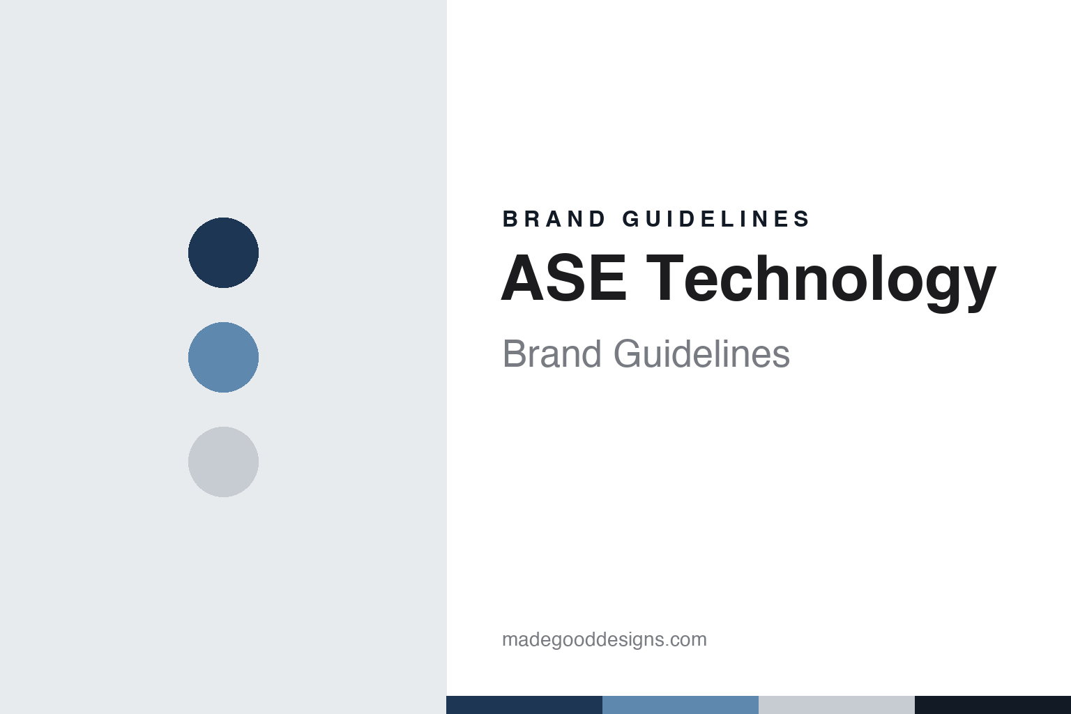
ASE Technology Brand Guidelines
The Kaohsiung packaging and test group behind ASE, SPIL and USI.
Aa
Two constants: an ASE navy, blue and wafer grey palette and an Engineered sans register. Abstract homage — not an ASE Technology product or mark; no package, logo or nameplate is reproduced.
Sun, moon and light
A Kaohsiung packaging firm from 1984.
ASE began in Kaohsiung, the port city in southern Taiwan, in 1984. English Wikipedia credits the brothers Jason Chang and Richard Chang with founding Advanced Semiconductor Engineering and opening its first factory there; Chinese Wikipedia names their mother, Chang Yao Hung-ying, as the founder, with Jason Chang as chairman. The group’s own website gives 1984 as its founding year and Jason Chang as its chairman.
The company’s Chinese name, 日月光 — “sun, moon and light” — was chosen by the Buddhist master Hsing Yun, Chinese Wikipedia says; he linked electricity and light with speed, and with something that can shine on very many people. English Wikipedia describes the company as a provider of independent semiconductor packaging and test services: it takes chips made by others and packages and tests them, the stage the trade calls outsourced semiconductor assembly and test.
Listings followed. Chinese Wikipedia says ASE listed on the Taiwan Stock Exchange in 1989 and in the United States in 2000, and that its testing subsidiary, ASE Test, listed on Nasdaq in 1996. In 2025 the group marked “25 years on the NYSE” on its own milestones page. Its factories in Kaohsiung are known by numbers — the Taipei Times described the K7 plant in 2013 as one of more than a dozen the company ran in the city’s Nanzih District.
Colour
Fan-out, flip chip and the holding company.
English Wikipedia lists ASE’s packaging methods as fan-out wafer-level packaging, wafer-level chip-scale packaging, flip chip, 2.5D and 3D packaging, system in package and copper wire bonding. It says ASE began volume production of wafer-level chip-scale packages in October 2001 and was among the first companies to mass-produce system-in-package parts, in 2004; Chinese Wikipedia adds that ASE has offered copper wire bonding since 2008. ASE also worked with AMD on 2.5D packaging from 2007, English Wikipedia says, and the two companies’ Fiji graphics processor was launched at the E3 games show in June 2015.
The group widened beyond packaging in 2010, when, Chinese Wikipedia says, ASE completed its purchase of USI, the Nantou electronics maker known in Chinese as 環隆電氣, taking it into system and module assembly. The larger step followed in 2016. English Wikipedia says ASE and Siliconware Precision Industries (SPIL), the Taichung packaging firm also founded in 1984, signed an agreement on 26 May 2016 to form a new holding company; Chinese Wikipedia dates the two boards’ approval of the share swap to 20 June 2016 and says Taiwan’s Fair Trade Commission cleared the deal the same year.
ASE Technology Holding listed on the Taiwan Stock Exchange on 30 April 2018, Chinese Wikipedia says, and the group’s milestones page records the listing that month in Taipei and New York. Conditions set by China’s commerce ministry kept ASE and SPIL operating separately, apart from research, until the restrictions were lifted in March 2020, according to both Chinese Wikipedia and the group. Today the holding company describes itself as combining ASE, SPIL and USI, with more than 95,000 employees and manufacturing in 15 countries, including Taiwan, China, South Korea, Japan, Malaysia, Vietnam, Mexico, the United States and Tunisia. In March 2025, Chinese Wikipedia says, ASE broke ground on new buildings for logistics and advanced testing in Kaohsiung’s Nanzih technology park, due for completion in 2028. The same month, it says, ASE bought the Taiwan subsidiary of Sumitomo Chemical, whose Nanzih site it plans to rebuild as a new plant. The group’s milestones page also records that it set up what it calls the first 5G millimetre-wave smart factory at ASE Kaohsiung in December 2020, and that it was named on CDP’s A List for climate and water in 2024.
Typography
Packaging and test.
Chip packaging and test companies sit between the chipmaker and the finished device. The trade calls them OSATs, for outsourced semiconductor assembly and test: they take silicon made by others, mount it, connect it, seal it and check that it works. Their customers are other technology companies, so they rarely speak to the public, and their imagery is built for engineers, buyers and investors.
That imagery leans on close-ups. Company pages and annual reports return again and again to macro shots of packaged chips and the substrates beneath them, to fine arcs of gold or copper wire bonds linking a die to its frame, and to wafers catching the light. Methods carry the names that a consumer brand would give to products: flip chip, fan-out, system in package, 2.5D and chiplet packaging.
The second register is the factory. Rows of test handlers, operators in white cleanroom suits, and long, low factory campuses in places such as Kaohsiung, Penang and Jiangsu stand for scale and reliability. Plants are often known by codes and numbers rather than names, and maps of sites across Asia, Europe and the Americas do much of the storytelling. Trade shows such as SEMICON are where these companies meet their customers face to face.
This guide sets out what can be checked about each company — who founded it, who owns it, where it works and what its record shows — and marks clearly what rests only on the company’s own word. The palettes and type here are our own interpretation, not the companies’ marks.
Aa
An engineered sans — the register of process charts and plant numbers. (Specimen set in IBM Plex Sans, a sans STAND-IN; NOT the ASE Technology logo.)
ASE Technology
The K7 case.
The group’s record includes a long environmental case. On 20 December 2013 the environmental protection bureau of what was then Greater Kaohsiung ordered ASE’s K7 plant to stop operating, the Taipei Times reported, after finding that acidic wastewater containing nickel had been discharged into the Houjin River; the bureau cited the Water Pollution Control Act. English Wikipedia says the bureau allowed K7 to resume operations in December 2014, after checking the company’s improvements to wastewater treatment.
The criminal case went back and forth. On 20 October 2014 the Kaohsiung District Court convicted four K7 employees and fined the company, Focus Taiwan reported, with suspended sentences. On 29 September 2015 the Taiwan High Court’s Kaohsiung branch reversed that ruling and acquitted the company and all five defendants, the Taipei Times reported, finding that the Waste Disposal Act did not apply. After the Supreme Court sent the case back, a retrial at the same branch in August 2017 again convicted four employees, with suspended sentences, in a ruling open to appeal, Storm Media reported; ASE said it respected the court’s decision. English Wikipedia also records that ASE built a water recycling plant in Kaohsiung, K14, which began trials in January 2015.
For a design guide, ASE Technology shows how a supplier whose work sits inside other companies’ chips presents itself through process names, plant numbers and a group structure. Compare Amkor, the Arizona packaging and test company that grew from ANAM in Korea, and AMD, ASE’s partner on 2.5D packaging. For this guide we use a harbour navy, a strait blue and a wafer grey with a sans, an unofficial interpretation; no product or logo is reproduced.
Explore & save
Keep ASE Technology’s identity on hand — save it to a board in the Made Good inspiration library.
ASE Technology identity set
Pin the ASE navy, blue and wafer grey palette and the Engineered sans register to your own board.