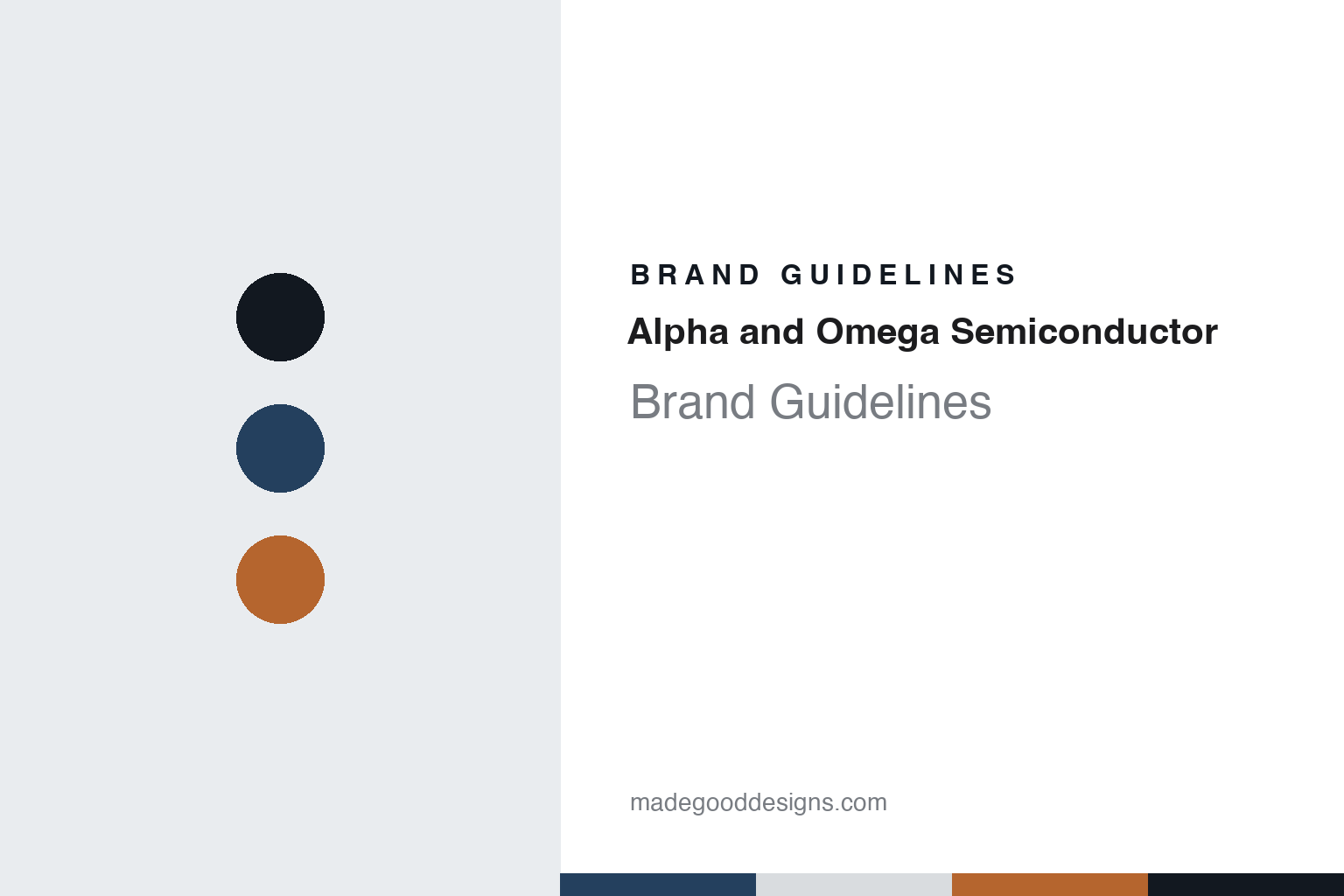
Alpha and Omega Semiconductor Brand Guidelines
Siliconix alumni, power MOSFETs and a joint venture in Chongqing.
Aa
Two constants: a navy, grey and copper palette and an engineered sans register. Abstract homage — not an Alpha and Omega Semiconductor product or mark; no chip, package or logo is reproduced.
From Siliconix
Three power-chip engineers and a Greek-letter name.
Alpha and Omega Semiconductor, which signs itself AOS, was founded in 2000. When it prepared to go public in April 2010, Renaissance Capital described it as founded “by a trio of engineers from power chip company Siliconix.” The company names Mike F. Chang as its founder. Its own biography of him says he worked at General Electric from 1974 to 1987 in product research and development, then held management roles at Siliconix, the power-semiconductor maker owned by Vishay Intertechnology, from 1987, serving as its executive vice president from 1998 to 2000.
Mike Chang ran AOS as chief executive from its founding until March 2023, the company says. Stephen C. Chang, who had been president since January 2021 and had earlier led its MOSFET product line and marketing, then became chief executive. Mike Chang was executive chairman until March 2025 and is now chairman of the board and executive vice president of strategic initiatives. The company’s press releases carry a Sunnyvale, California dateline, and its website shows its Sunnyvale headquarters.
The stock-market debut came in spring 2010. Renaissance Capital reported on 29 April 2010 that the offering had priced and that the shares would trade on Nasdaq under the symbol AOSL, where the parent company, Alpha and Omega Semiconductor Limited, is still listed. In its preview a few days earlier, the research firm described AOS as a supplier of power-management chips for notebook computers, flat-panel displays, mobile battery packs and digital cameras, built on proprietary process and packaging technology and what it called a “semi-fabless” model, in which testing and packaging for many of its chips were done in-house.
The name pairs the first and last letters of the Greek alphabet. In its own copy the company uses the three-letter AOS, and its website address uses the letters “aosmd” rather than the full name.
Colour
MOSFETs, power ICs and packaging.
AOS describes itself as a designer, developer and global supplier of discrete power devices, wide-bandgap power devices, power-management ICs and modules. In its own summary the portfolio runs from power MOSFETs and IGBTs to silicon-carbide and gallium-nitride devices, and it says its difference lies in combining discrete and IC process technology, product design and advanced packaging know-how in one company. It lists its target markets as high-volume equipment such as personal computers, graphics cards, AI servers and automotive electronics.
Packaging is a recurring theme in its announcements. In a press release dated 7 July 2026, AOS introduced AmpStack, a DFN 6×5 package in which two MOSFETs are stacked vertically to form a high-side and low-side pair, a half-bridge, inside one housing, with a clip connecting the switch node and a Kelvin sense pin for the gate drive. In September 2026 it announced a 600-volt superjunction MOSFET family called αMOS E2, and in April 2026 a protected DrMOS family aimed at AI servers and graphics processors. Its newsroom shows it exhibiting at PCIM in Nuremberg in June 2026 and at electronica in Munich in November 2026.
Manufacturing is split between its own fab and partners. The company says its wholly owned subsidiary Jireh Semiconductor is its in-house wafer fab, in Hillsboro, Oregon. In March 2016, Semiconductor Digest reported, AOS had a facility in Shanghai for assembly and testing; under its Chinese joint-venture plan it intended to move most of that assembly and test equipment to a new plant, keeping Shanghai as a centre for supply-chain management, technology development and high-value production.
That joint venture shaped the following decade. AOS signed a definitive agreement in March 2016 with two strategic investment funds owned by the Municipality of Chongqing to build a power-semiconductor packaging, testing and wafer-fabrication facility in the city’s Liangjiang New Area, Semiconductor Digest reported. AOS was to own 51 percent and the Chongqing funds 49 percent, subject to approval by the Chinese authorities. Packaging production was expected to start in mid-2017, with a 12-inch wafer fab planned for the longer term.
Typography
How power-chip makers present themselves.
Analog and power chipmakers sell parts that most people never see. Their products sit inside chargers, cars, motor drives and power supplies, usually as small black packages soldered to a board, so the industry’s visual language has to make something tiny and hidden look solid and precise. The usual answer is the macro photograph: a packaged chip or a power module shot close up against a dark or plain ground, its leads and markings sharp and its edges lit like an object in a catalogue.
Materials are the second subject. Makers that work with silicon carbide tend to show the wafer itself, a thin disc that often looks faintly green or amber under studio light, while gallium-nitride and silicon makers show wafers patterned with rows of dies. These images stand in for the factory, which tends to appear as clean-room suits and wafer carriers rather than as a building.
The third subject is the application. Power-chip makers lean heavily on electric-car chargers, inverters, solar installations and data-centre racks, because those are where their parts do visible work. Closer to the engineer, the pictures shift to evaluation boards on lab benches, probes and cables, and oscilloscope traces showing a clean switching edge — an image that speaks to the people who will design the chip in.
Trade shows complete the picture. Europe’s electronica in Munich and PCIM in Nuremberg, and APEC in the United States, are where many of these companies set out their stands, demonstration boards and new packages each year. In each of these settings the hardware and the technical data are meant to carry the message, with the brand kept to a name on the stand and the board.
Aa
An engineered sans for a company that writes itself as three capitals. (Specimen set in Archivo, a sans STAND-IN; NOT the Alpha and Omega Semiconductor logo.)
AOS
A partner, not a parent, in Chongqing.
By 2025 AOS no longer controlled the Chongqing venture. When it signed an equity-transfer agreement on 14 July 2025, Panabee reported, AOS held 39.2 percent of the joint venture and agreed to sell about 20.3 percent, roughly half of that holding, while keeping access to the venture’s wafer, assembly and test capacity under existing supply agreements. Benzinga reported on 13 May 2026 that the sale, between Alpha & Omega Semiconductor (Shanghai) and SIMIC Holdings, was completed when the final instalment arrived on 11 May 2026. The venture still runs a power-semiconductor packaging, testing and 12-inch wafer-fabrication plant in Chongqing.
The result is a company with an American listing and headquarters, its own wafer fab in Oregon, operations in Shanghai and a minority stake in a Chinese manufacturing partner. Its leadership has been continuous: the founder still chairs the board, and the chief executive, chief operating officer and head of worldwide sales all rose through the company, according to its own leadership page.
Visually, AOS leans on the short form. The three capitals appear in its domain and press releases, “AO” opens part numbers such as the AOPL66801, and the αMOS product name carries the Greek letter alpha from the full company name. Its announcements are technical and specific, built around package outlines, voltage classes and application areas such as AI servers, notebooks and electric-vehicle powertrains rather than lifestyle imagery, and its website is organised by products, applications and design support.
For a design guide, Alpha and Omega Semiconductor shows how a power-chip maker can carry a long Greek-letter name and a three-letter abbreviation side by side, and let packaging innovations do the visual talking. Compare onsemi, another power-semiconductor maker with deep American roots, and Monolithic Power Systems, a fellow power-management specialist. For this guide we use a wafer navy, die grey and copper with an engineered sans, an unofficial interpretation; no product or logo is reproduced.
Explore & save
Keep Alpha and Omega Semiconductor’s identity on hand — save it to a board in the Made Good inspiration library.
Alpha and Omega Semiconductor identity set
Pin the navy, grey and copper palette and the engineered sans register to your own board.