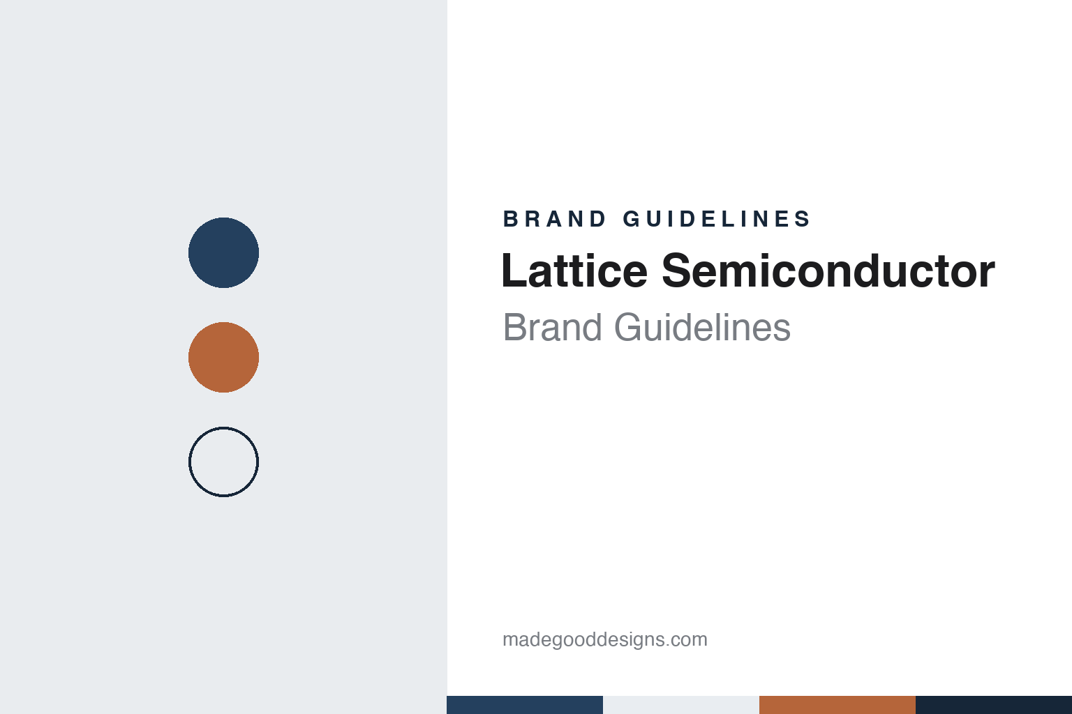
Lattice Semiconductor Brand Guidelines
The Silicon Forest maker of small, low-power programmable chips.
Aa
Two constants: a Lattice Semiconductor slate and copper palette and an Engineered sans register. Abstract homage — not a Lattice Semiconductor product or mark; no chip, logo or package marking is reproduced.
Silicon Forest
Three founders and an Oregon start.
Lattice Semiconductor was founded on 3 April 1983 in Oregon by C. Norman Winningstad, Rahul Sud and Ray Capece, English Wikipedia says, with money from Winningstad and the investors Harry Merlo, Tom Moyer and John Piacentini. It was incorporated in Oregon that year and reincorporated in Delaware in 1985. The company’s own “About” page puts its founding in “Oregon’s Silicon Forest,” the name given to the cluster of technology firms west of Portland.
The start was rough. Sud left as president in December 1986, and in July 1987 the young company entered Chapter 11 bankruptcy reorganisation. It came out after 62 days, English Wikipedia records, and moved from its first base in an unincorporated area near Beaverton to a smaller building in Hillsboro, where it is still headquartered. Over the following year it shrank from 140 to 64 employees while its sales grew.
Cyrus Tsui became chief executive in 1988, and on 9 November 1989 Lattice listed its shares on Nasdaq after an initial public offering; it still trades there under the symbol LSCC. Winningstad left as chairman in 1991.
The company has a curious footnote in the history of its region’s name. Lattice registered “Silicon Forest” as a trademark for semiconductor devices in 1985, and in 1995 tried to assert rights in the term more widely; according to English Wikipedia, it later conceded that it could not stop others using the phrase as an ordinary noun. In 1996 it began to double the size of its Hillsboro headquarters.
Colour
Programmable logic, kept small.
Lattice designs field-programmable gate arrays, or FPGAs — chips whose logic the customer configures after manufacture — along with older programmable logic devices and programmable power- and clock-management parts. “We design and develop programmable products, which allow the end customer to determine functionality,” its website says. For manufacturing, English Wikipedia records that in July 2012 Lattice announced a foundry agreement with the Taiwanese chipmaker United Microelectronics Corporation.
Its range was built partly through acquisitions. Lattice bought Integrated Intellectual Property, a Santa Clara design-IP firm, in March 2001; the FPGA division of Agere in 2002; SiliconBlue, announced in December 2011; and Silicon Image in March 2015, after which it moved its headquarters to downtown Portland, before returning to its Hillsboro campus in 2019. In November 2021 it bought Mirametrix, a computer-vision software company.
The modern line-up is organised as platforms. The company names the Lattice Nexus platform for small FPGAs, the Lattice Avant platform for mid-range FPGAs and the long-running MachXO family, with design software called Radiant and Propel; English Wikipedia also lists the older Diamond tool. Around them sit “solution stacks” aimed at particular markets — sensAI for machine learning in connected devices, mVision for machine vision, Automate for factories, Sentry for security and Drive for cars, according to English Wikipedia.
The company describes itself as “the low power programmable leader” and says it is “the #1 supplier of small FPGAs worldwide, with the largest installed base in the industry”; those are its own claims. It also promises “20+ year product longevity” for its FPGAs. In 2011, English Wikipedia says, Lattice ranked third among FPGA makers and second in simpler programmable devices.
Typography
Design and documentation.
A fabless chip designer has an unusual problem for a brand: its product is a small, dark square that most buyers never see. The company designs the chip, an outside foundry makes the wafers, and the finished part disappears inside someone else’s phone, television, router or car. The visual language of the category grows out of that gap between what the company makes and what anyone can look at.
One answer is the rendering. Chips appear floating above circuit-board landscapes, lit from below, with traces running off toward the horizon like roads seen from the air. Another is the die photograph: a close view of the silicon itself, often tinted in false colour so that memory blocks, processor cores and interfaces read as separate districts on a map.
A third answer is to show the products the chip ends up in. Reference designs — earbuds, security cameras, smart speakers, displays, small smart-home gadgets — let a designer point to a finished object without claiming it as its own. Developer kits and evaluation boards, photographed on desks next to laptops and cables, speak to the engineers who choose components.
The calendar matters too. Much of the category’s public presentation happens at trade shows such as CES in Las Vegas, Computex in Taipei, Embedded World in Nuremberg and the Hot Chips conference, where booths, demo walls and technical papers carry the brand. Many press releases follow the same rhythm, dated from headquarters and timed to a show. The guides that follow look at how individual companies work within these conventions, and at what can be documented about each one.
Aa
An engineered sans for a programmable-logic company. (Specimen set in IBM Plex Sans, a sans STAND-IN; NOT the Lattice Semiconductor logo.)
Lattice Semiconductor
A blocked sale and a firmware purchase.
Lattice’s later history includes two episodes with governments. In 2004, English Wikipedia says, it settled charges by the United States government that it had illegally exported certain technologies to China. In November 2016 the private-equity firm Canyon Bridge Capital Partners agreed to buy the whole company; on 13 September 2017 a presidential order, published in the Federal Register on 18 September, prohibited the proposed acquisition by China Venture Capital Fund Corporation Limited and the related Canyon Bridge entities, on national-security findings under section 721 of the Defense Production Act.
Lattice stayed independent. In 2018 the activist investor Lion Point Capital took a stake and three new independent directors joined the board; the same year Jim Anderson, formerly of AMD, became chief executive, and the company turned its focus to low-power FPGAs. Anderson left in June 2024, and Ford Tamer was named chief executive on 16 September 2024. After AMD completed its purchase of Xilinx in February 2022, English Wikipedia says, Lattice became the last fully independent major maker of FPGAs.
Its largest step since came in 2026. Lattice announced an agreement to buy AMI — American Megatrends, the platform-firmware company — on 4 May 2026 and completed the purchase on 27 July 2026, its press release says. AMI now runs as a business unit called “AMI, a Lattice Company,” whose products include the Aptio, MegaRAC and Tektagon firmware lines, and Lattice now describes the pair as offering “the most complete secure management and control platform in the industry,” a claim made in the company’s own words.
For a design guide, Lattice Semiconductor shows how a component maker with no consumer product can still build a name around one idea — small, low-power programmable chips — and a place, the Silicon Forest. Compare AMD, which owns the Xilinx FPGA business, and Synaptics, another American fabless chip designer. For this guide we use a slate blue and a copper with a sans, an unofficial interpretation; no product or logo is reproduced.
Explore & save
Keep Lattice Semiconductor’s identity on hand — save it to a board in the Made Good inspiration library.
Lattice Semiconductor identity set
Pin the Lattice Semiconductor slate and copper palette and the Engineered sans register to your own board.