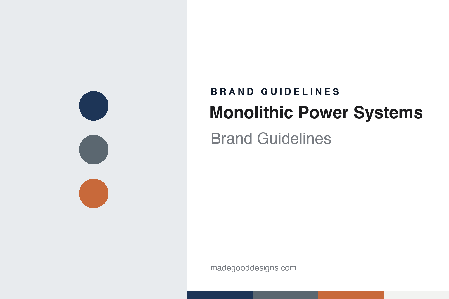
Monolithic Power Systems Brand Guidelines
Michael Hsing’s 1997 fabless power-chip maker.
Aa
Two constants: a navy, slate and copper palette and an engineering sans register. Abstract homage — not a Monolithic Power Systems product or mark; no chip, board, logo or nameplate is reproduced.
Founded in 1997
An engineer’s process technology and a fabless plan.
Monolithic Power Systems, usually shortened to MPS, was founded in 1997 by Michael Hsing, who still runs it. The company’s annual report for 2025, filed with the US Securities and Exchange Commission, names him as president, chief executive and chairman of the board, and says that before founding MPS he was a senior silicon technology developer at several analog chip companies, where he developed and patented key technologies. In a December 2008 profile, the trade magazine Electronic Design named two of those earlier employers as Supertex and Micrel, and described Hsing as an inventor of high-speed, high-power semiconductor process technology.
The company was built around a process rather than a factory. Electronic Design described MPS in 2008 as a high-performance analog semiconductor company headquartered in San Jose, California, with more than 550 employees in design centres and sales offices in Japan, Europe, China, Korea, Taiwan and the United States. The focal point of its business, the magazine wrote, was a proprietary BCD Plus process, implemented at standard CMOS foundries, that combines BiCMOS signal transistors with an efficient DMOS power transistor, so that power-management circuits can be built as single chips.
Hsing took the company public in November 2004, Wikipedia and the company’s filings say, and its shares trade on Nasdaq under the symbol MPWR. In 2008 its range, as Electronic Design listed it, ran from DC-DC converter ICs and LED drivers to backlight inverters for LCD screens and Class D audio amplifiers.
Colour
Fabless, but with its own process.
MPS has never run its own wafer fab. Its 2025 annual report calls it “a fabless global company” providing semiconductor-based power electronics, and explains the difference it claims from many other fabless firms: rather than using the standard process technologies and design rules of its foundries, it has developed its own process and packaging technologies and works with foundry partners to install them on equipment in their plants for use on its behalf. Electronic Design described the same arrangement in 2008.
The filing is specific about where its chips are made. MPS says its wafers are manufactured at foundries in China, Taiwan, South Korea and Singapore. Wafer sort and final test take place at facilities that it and its partners use in China, Taiwan, Singapore, Malaysia and South Korea, and independent subcontractors assemble and package the chips in China, Taiwan, Malaysia and South Korea. The company says its largest testing facilities are in Chengdu, China, and that they are certified to ISO 14001 and ISO 45001.
Asia is also where it has been adding engineering. On 10 March 2026 MPS opened its first engineering and test centre in Penang, Malaysia, according to a press release from InvestPenang, the Penang state government’s investment agency, which said the centre would also serve as the company’s Malaysian headquarters and support its testing capacity.
Typography
How power chipmakers present themselves.
Analog and power chipmakers sell parts that most people never see. Their products sit inside chargers, cars, motor drives and power supplies, usually as small black packages soldered to a board, so the industry’s visual language has to make something tiny and hidden look solid and precise. The usual answer is the macro photograph: a packaged chip or a power module shot close up against a dark or plain ground, its leads and markings sharp and its edges lit like an object in a catalogue.
Materials are the second subject. Makers that work with silicon carbide tend to show the wafer itself, a thin disc that often looks faintly green or amber under studio light, while gallium-nitride and silicon makers show wafers patterned with rows of dies. These images stand in for the factory, which tends to appear as clean-room suits and wafer carriers rather than as a building.
The third subject is the application. Power-chip makers lean heavily on electric-car chargers, inverters, solar installations and data-centre racks, because those are where their parts do visible work. Closer to the engineer, the pictures shift to evaluation boards on lab benches, probes and cables, and oscilloscope traces showing a clean switching edge — an image that speaks to the people who will design the chip in.
Trade shows complete the picture. Europe’s electronica in Munich and PCIM in Nuremberg, and APEC in the United States, are where many of these companies set out their stands, demonstration boards and new packages each year. In each of these settings the hardware and the technical data are meant to carry the message, with the brand kept to a name on the stand and the board.
Aa
A clean engineering sans for a power-chip maker. (Specimen set in Manrope, a sans STAND-IN; NOT the Monolithic Power Systems logo.)
MPS today
Power chips for storage, data centres and cars.
The range has grown well beyond the 2008 list. The annual report names its key product families as DC-DC and AC-DC converters, driver MOSFETs, power-management ICs and lighting-control products, among others. MPS sells into six end markets: storage and computing, enterprise data, automotive, communications, consumer and industrial. It says storage and computing was its largest market in 2025, closely followed by enterprise data, which covers servers, workstations and artificial-intelligence systems. Most sales go through third-party distributors and value-added resellers, supported by applications engineers who work directly with customers’ own engineers.
The filing also spells out what those markets mean in practice. In cars, MPS lists driver-assistance systems, infotainment, body electronics and lighting; in communications, network infrastructure, satellite communications and optical modules; in consumer products, home appliances, gaming and smart TVs. Its DC-DC converters, the company says, convert and control voltages in systems ranging from CPU servers and memory to infotainment units, home appliances and satellite links, and it plans to keep adding products within its existing families as well as in new categories.
The company states its mission as reducing “energy and material consumption to improve all aspects of quality of life”, and the 2026 Penang release repeated that wording alongside the founding story of Hsing and three core strengths in system-level knowledge, semiconductor expertise and proprietary technologies.
Where MPS is based is less simple than for most listed companies. Its SEC filings from February 2026 give a principal executive office in West Palm Beach, Florida, but a footnote says the company has operations in multiple locations in the US, Europe and Asia and has not identified a single location as its headquarters, giving the address only to comply with SEC requirements. MPS joined the S&P 500 in February 2021 and the Nasdaq-100 in December 2025, Wikipedia says.
For a design guide, Monolithic Power Systems shows a chip company whose identity rests on an engineer’s process technology and a fabless model rather than a factory or a single home town. Compare it with Analog Devices and Texas Instruments, two other analog chipmakers. For this guide we use a deep navy, slate and a copper orange with a sans, an unofficial interpretation; no product or logo is reproduced.
Explore & save
Keep Monolithic Power Systems’s identity on hand — save it to a board in the Made Good inspiration library.
Monolithic Power Systems identity set
Pin the Monolithic Power Systems navy, slate & copper palette and the engineering sans register to your own board.