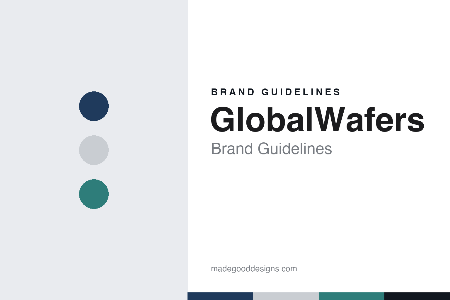
GlobalWafers Brand Guidelines
A Hsinchu spin-off that grew into a wafer group by acquisition.
Aa
Two constants: a navy, silver and teal palette and a technical sans register. Abstract homage — not a GlobalWafers product or mark; no wafer, logo or nameplate is reproduced.
A carve-out
A solar company’s wafer division becomes a company of its own.
GlobalWafers Co., Ltd. is a silicon wafer maker headquartered in the Hsinchu Science Park in Taiwan. Its roots are in Sino-American Silicon Products, known as SAS, whose semiconductor business the company says was founded in the science park in 1981. SAS later moved into solar cells and modules as well, and on 1 October 2011 it completed the carve-out of its semiconductor division as a separate company, GlobalWafers, according to Chinese-language Wikipedia and the company’s own profile. The company still describes SAS as its parent.
The new company inherited two earlier moves. SAS set up a subsidiary in mainland China, known as SST, in 1999 to supply 4-inch to 8-inch wafers, and on 1 April 2008 it bought GlobiTech, an American maker of epitaxial wafers; both became wholly owned GlobalWafers subsidiaries at the carve-out, the company says. It credits GlobiTech with bringing epitaxial expertise and direct contact with large chipmakers.
Growth then came largely by acquisition. In April 2012 GlobalWafers completed the purchase of the silicon wafer business of Japan’s Covalent Materials, Chinese-language Wikipedia says; the company says the unit was renamed GlobalWafers Japan on 1 January 2013. The shares were listed on the Taipei Exchange, Taiwan’s over-the-counter market, on 25 September 2015, the same source says. On 1 July 2016 GlobalWafers completed the purchase of the semiconductor business of Topsil of Denmark, which it describes as a pioneer of neutron-transmutation-doped float-zone silicon, used in cars and high-power devices. In December 2016 it completed its takeover of SunEdison Semiconductor, a US wafer maker; English Wikipedia says that business was renamed MEMC and remains a wholly owned subsidiary.
Colour
From 3-inch wafers to a Texas campus.
GlobalWafers says it makes silicon wafers from 3 inches to 12 inches across, with complete production lines running from ingot growth through slicing, etching, polishing and epitaxy. It names its higher-value products as epitaxial, polished, diffusion, annealed, SOI, float-zone and compound wafers, and lists power management, automotive, IT and MEMS among the uses. The company describes itself as Taiwan’s largest and the world’s third-largest wafer maker; English Wikipedia also places it third as of 2022.
The acquisitions left it with factories in several countries. English Wikipedia says it operates in South Korea through MEMC Korea, where a second fab opened in 2019. Its Italian subsidiary, MEMC S.p.A., received research and development subsidies in July 2024, the company says, and in October 2025 it launched FAB300 in Novara, Italy, which it calls a fully integrated 300 mm wafer plant. The electronics trade site Evertiq reported in May 2025 that GlobalWafers operates 18 sites in nine countries.
The newest plant is in the United States. GlobalWafers decided in May 2022 to build its flagship plant there and broke ground in Sherman, Texas, in December 2022, Evertiq reported on 21 May 2025. The plant, GlobalWafers America, held its grand opening on 15 May 2025; the company calls it “the industry’s most advanced fully integrated 300mm semiconductor wafer facility.” At the opening, chairperson Doris Hsu announced a further expansion that adds phases three and four to a campus designed for up to six phases, Evertiq reported, adding that the project receives federal support through the CHIPS program. The company says it signed its final agreement with the US Department of Commerce in December 2024.
English Wikipedia describes the Sherman plant as the first of three planned there, and notes that the company billed it at the opening as the “new epicenter of semiconductor manufacturing in North America.” Those are the company’s words, not an independent assessment.
Typography
Wafers and chip materials.
Silicon-wafer and chip-materials makers sell to a small number of very large customers, and their public image is built for engineers, investors and recruits rather than shoppers. Most of what they make never reaches a consumer’s hand: a polished wafer, a bottle of photoresist or a photomask is used up or hidden inside a chip long before anything is sold in a shop.
Their pictures tend to come from the factory floor. Corporate reports and websites in this field favour mirror-polished silicon wafers catching the light of a cleanroom, cylindrical crystal ingots drawn slowly out of a furnace, photolithography bays lit in amber to protect light-sensitive resists, and racks of high-purity chemical bottles. People appear mostly as technicians in full-body cleanroom suits, often called bunny suits, with only their eyes showing.
Names in this group often record a history. Shin-Etsu joins two old Japanese provinces, and SUMCO is an acronym of the company formed by a 1999 merger. The palettes in these guides are our own interpretations, not official colours.
The industry meets at its trade shows. SEMICON West in the United States, SEMICON Taiwan in Taipei and SEMICON Japan in Tokyo bring wafer, chemical and equipment suppliers onto the same floor as chipmakers, and booths there show the same vocabulary of wafers, ingots and cleanroom imagery. This guide sets out what can be checked about each company — who founded it, who owns it, where it makes its products — and marks clearly what rests only on the company’s own word.
Aa
A precise, engineered sans for a wafer group. (Specimen set in IBM Plex Sans, a sans STAND-IN; NOT the GlobalWafers logo.)
GlobalWafers
The Siltronic bid that lapsed, and what followed.
One chapter of the company’s history is a deal that did not happen. In December 2020 GlobalWafers announced a takeover offer for Siltronic, the Munich wafer maker, through its German subsidiary GlobalWafers GmbH; the company says 70.27 percent of the shares had been tendered when the extended acceptance period ended on 1 March 2021. China’s market regulator said on 21 January 2022 that it would give conditional approval, Reuters reported, but Germany’s economy ministry did not complete its investment review before the deadline of 31 January 2022, and the offer lapsed. A ministry spokesperson said not all review steps could be completed, in particular the review of the Chinese antitrust approval, granted only the week before; the ministry said it would review again if GlobalWafers made a new attempt (Reuters, via Euronews, 1 February 2022; Taipei Times, 2 February 2022).
GlobalWafers said in February 2022 that, having failed to meet all the conditions of the acquisition, it planned a major greenfield expansion, according to its own milestones; the Texas plant followed. It kept a stake in Siltronic. German Wikipedia lists Sino-American Silicon Products with 13.67 percent of Siltronic as of December 2025, and in January 2024 GlobalWafers GmbH priced exchangeable units that can be exchanged for Siltronic shares, the company says.
One practical note for anyone looking the company up: its website sits at sas-globalwafers.com, under the parent’s initials, while the plain globalwafers.com address is a parked domain listed for sale and is unrelated to the company.
For a design guide, GlobalWafers shows how a spun-off division can build an international group through acquisitions while keeping its parent’s initials in its web address. Compare Siltronic, the Munich wafer maker it once tried to buy, and SUMCO, a Japanese wafer maker. For this guide we use a deep navy, a wafer silver and a teal with a sans, an unofficial interpretation; no product or logo is reproduced.
Explore & save
Keep GlobalWafers’s identity on hand — save it to a board in the Made Good inspiration library.
GlobalWafers identity set
Pin the GlobalWafers navy, silver and teal palette and the technical sans register to your own board.