AT&S Brand Guidelines
From Austria’s state electronics plants to IC substrates in Chongqing and Kulim.
Aa
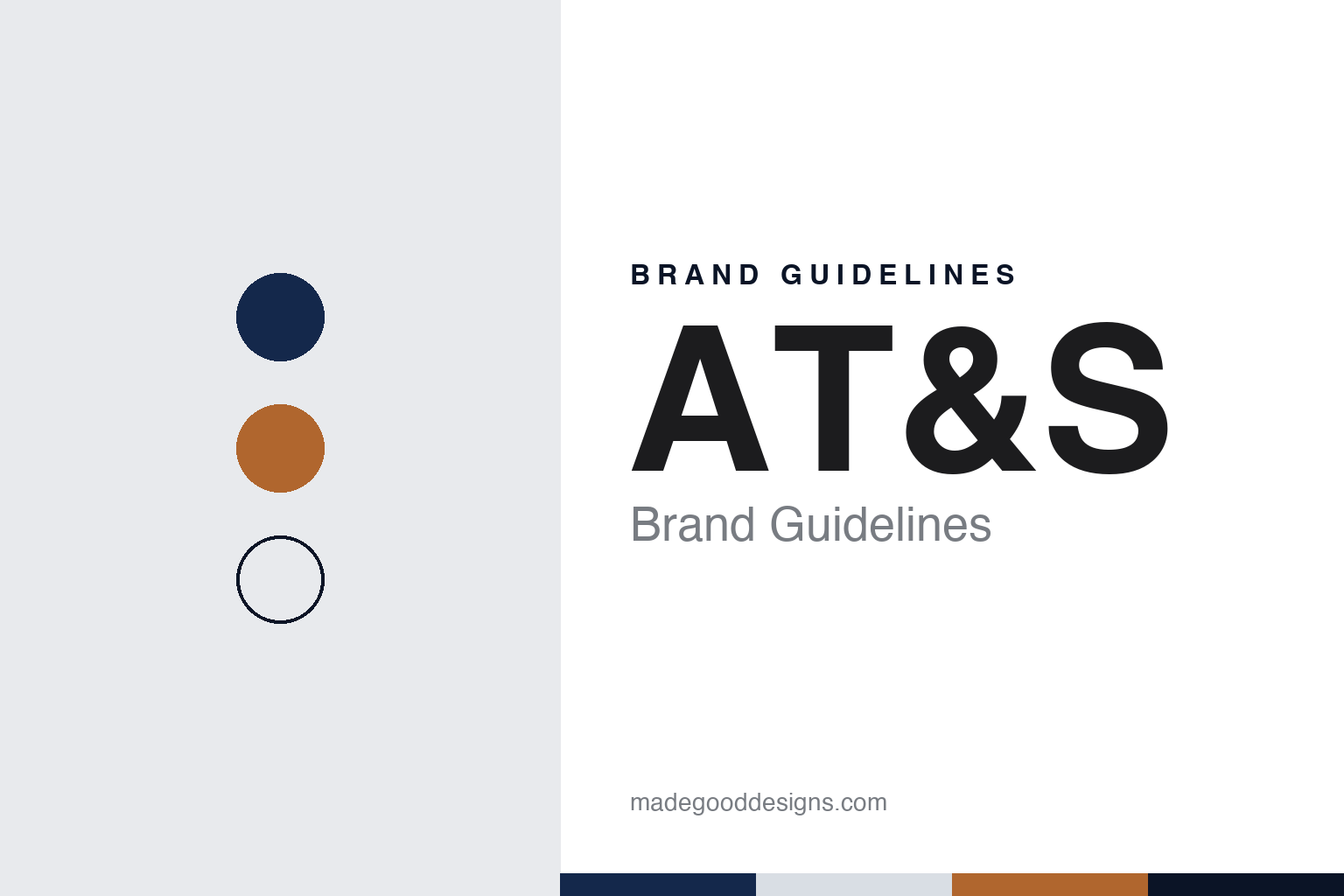
Two constants: a deep navy, copper and cool grey palette and a condensed sans register. Abstract homage — not an AT&S product or mark; no board, logo or nameplate is reproduced.
Austria Technologie & Systemtechnik
Three state-owned plants merged in 1987.
AT&S, in full AT & S Austria Technologie & Systemtechnik Aktiengesellschaft, was formed in 1987 out of Austria’s state-owned industry. German Wikipedia says the company grew from three units founded in the 1970s: a Körting Elektronik site at Fehring, which Elin had taken over in 1979 and renamed Steirische Elektronik, making televisions and circuit boards; a branch plant of Eumig at Fohnsdorf; and a Voest-Alpine site at Leoben. From 1990 its parent was E+E Leiterplattenholding, and until 1994 it belonged to the state holding company ÖIAG. The company’s own timeline describes its 1987 founding as a merger of several companies in state-owned Austrian industry.
Privatisation came in November 1994, when the business was sold to a consortium of the investors Androsch, Dörflinger and Zoidl, German Wikipedia says; the company’s timeline names the same three buyers. In 1995 it became a joint-stock company. The headquarters has stayed in Leoben, in Styria.
Expansion abroad followed quickly. AT&S bought Indal Electronics at Nanjangud, near Mysuru in southern India, in 1998 according to German Wikipedia and in 1999 according to the company, which describes it as the largest Indian PCB factory at the time and says it is now AT&S India. The shares were listed on the Frankfurt Stock Exchange from 1999. Production began in Shanghai in 2002, German Wikipedia says, while the company dates its Shanghai expansion to 2001. In 2006 AT&S bought the Korean flexible-board maker Tofic, later AT&S Korea, and in 2008 it moved its listing to the Vienna Stock Exchange, where it remains.
Colour
From phone boards to IC substrates.
AT&S makes high-end printed circuit boards and IC substrates. German Wikipedia describes it as a maker of IC substrates and HDI microvia boards supplying mobile phone, automotive, industrial and medical electronics companies. Its customer history is set out there in some detail: Nokia was a customer from 1992, joined by Motorola, Siemens and Sony Ericsson; as business with Nokia declined, RIM and then Apple took its place, and the Shanghai and Chongqing plants have appeared on Apple’s list of its top 200 suppliers since 2008 and 2020 respectively. In 2015 AT&S also supplied boards to Fairphone, both Wikipedia editions say.
The Austrian plants were given narrower roles. From 2005 Fohnsdorf specialised in rigid-flex boards and Fehring in flexible boards, German Wikipedia says, and in 2006 Fohnsdorf was closed and merged into Leoben. Since 2009, according to both the company and German Wikipedia, the Austrian factories have concentrated on premium niches in the automotive and industrial sectors, while Shanghai concentrates on high-end mobile devices. A plant at Klagenfurt operated until 2013.
The turn to substrates began in Chongqing. Construction started there in 2011 on what was planned as another HDI plant, but German Wikipedia says the plan changed at the end of 2012, when AT&S won Intel as a customer for 2013; the company’s timeline says only that it entered the IC substrate business in 2013 “in cooperation with a leading semiconductor manufacturer.” Series production of IC substrates began in Chongqing in 2016, and the first phase was completed in June 2017, German Wikipedia says, with one plant making substrates for desktop and notebook processors and another making substrate-like boards by the mSAP process for mobile devices. The company dates the start of a third Chongqing factory for IC substrates to 2019.
Typography
Boards and substrates.
Printed circuit boards sit inside almost every electronic product, yet the companies that make them rarely sell to the public. Their brands are written for engineers, buyers and investors, and their pictures tend to come from a short, shared list: a green or black board lit from the side so that its copper traces catch the light, a macro shot of vias and solder pads, or the gold-plated contact fingers along a board’s edge.
The factory is the other recurring subject. Board makers show long plating lines, rows of drilling machines, clean rooms and inspection stations, because scale and process are what they are selling. Flexible circuits get their own pose — a thin amber strip curled over a fingertip — while makers of IC substrates, the fine-lined carriers that sit between a chip and its board, tend to show close-ups of dense, glossy panels rather than finished products.
Names are often short and technical: TTM Technologies, for one, says its initials stand for “time-to-market.” Few makers publish formal colour standards, so the palettes in these guides are our own reading of the trade’s materials — the green of solder mask, the dark of laminate, the warm metal of copper and gold — rather than any company’s specification.
The trade meets at its own shows. The TPCA Show in Taipei gathers Taiwan’s board and substrate makers and their suppliers, and the electronica fairs, in Munich and elsewhere, bring board makers together with the component and equipment trade; TTM Technologies, for one, announced that it would exhibit at electronica India in Bangalore in 2026. The makers in this guide are spread across the United States, Taiwan, mainland China, Japan and Europe, and several of them run plants in more than one of those places.
Aa
A narrow, engineered sans for a company whose name is an abbreviation. (Specimen set in Barlow Semi Condensed, a sans STAND-IN; NOT the AT&S logo.)
AT&S
Kulim, Leoben and a sale in Korea.
The largest recent projects are in Malaysia and at home. German Wikipedia says AT&S announced in June 2021 that it would build an IC substrate plant in Malaysia, and the company dates the groundbreaking at Kulim, in Kedah, to 2021. The New Straits Times reported in January 2024 that the campus in the Kulim Hi-Tech Park was officially open after just over two years of construction, and that it would start delivering high-end IC substrates for AMD’s data centre processors towards the end of that year; AT&S board member Ingolf Schroeder told the paper that Malaysia had been chosen in 2021 for the company’s first facility in Southeast Asia.
In Leoben, the foundation stone for a European competence centre with series production of IC substrates was laid in March 2022, and the new plant, known as Hinterberg 3, opened in June 2025, German Wikipedia says. English Wikipedia says that with it AT&S became the first and only company in Europe with local capabilities for developing and producing IC substrates.
The group also shrank in one place. On 23 September 2024 AT&S signed an agreement to sell AT&S Korea, with its plant at Ansan, to the Italian company SO.MA.CI.S., and the company’s timeline records the sale under 2025. English Wikipedia now lists six production sites: Leoben and Fehring in Austria, Nanjangud in India, Chongqing and Shanghai in China, and Kulim in Malaysia. Michael Mertin became chief executive on 1 May 2025.
The company also claims a deeper lineage. Its history page introduces Paul Eisler, whom it calls the inventor of the printed circuit board and notes was born in Vienna, and says that as an Austrian company AT&S has a direct historical link to the origins of the PCB.
For a design guide, AT&S shows a company whose name is an abbreviation of a long German one, held together by the ampersand. Compare Würth Elektronik, a German circuit-board maker, and Intel, an IC substrate customer from 2013 according to German Wikipedia. For this guide we use a deep navy, copper and a cool grey with a condensed sans, an unofficial interpretation; no product or logo is reproduced.
Explore & save
Keep AT&S’s identity on hand — save it to a board in the Made Good inspiration library.
AT&S identity set
Pin the AT&S deep navy, copper and cool grey palette and the condensed sans register to your own board.