Nan Ya PCB Brand Guidelines
A plastics division that grew into an IC substrate maker.
Aa
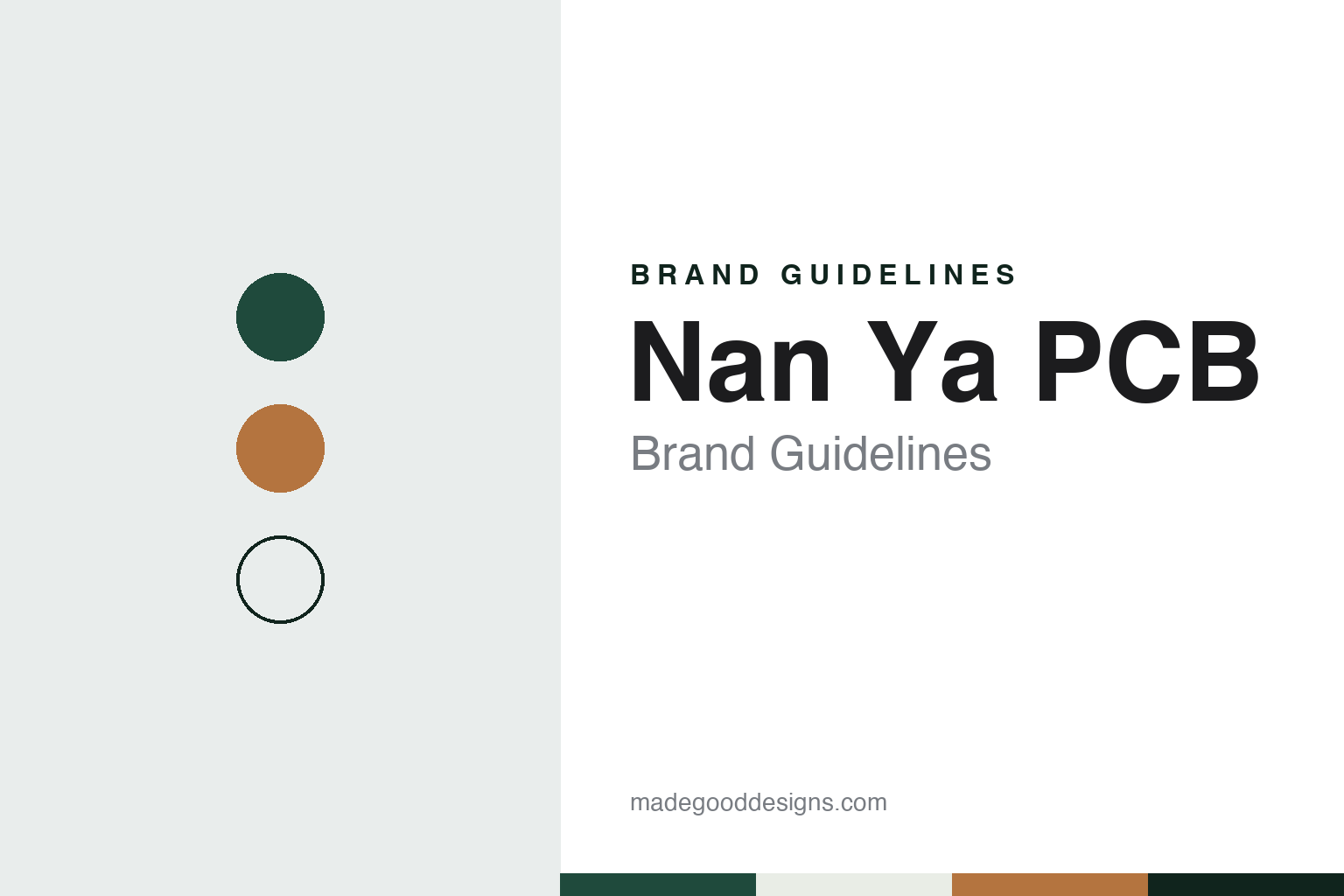
Two constants: a laminate green and copper palette and an engineering sans register. Abstract homage — not a Nan Ya PCB product or mark; no board, logo or nameplate is reproduced.
A Plastics Division
Circuit boards inside a plastics group.
Nan Ya PCB began inside a plastics company. The company says its circuit-board business started in 1985 as the PCB division of Nan Ya Plastics, and that in October 1997 it was set up as a separate subsidiary through a reinvestment by its parent, with Yung-Ching Wang as chair and Chia-Fung Chang as president. It began operating on its own as Nan Ya Printed Circuit Board Corporation in 1998, and it still uses the shorter Nan Ya PCB name on its website.
The parent matters to the story. Nan Ya Plastics is part of the Formosa Plastics Group; Taiwan News described it in November 2025 as a key subsidiary of the group, with operations that run from plastics processing and polyester to electronics. The same report, citing the financial news site MoneyDJ, said Nan Ya Plastics is one of the world’s largest makers of copper-clad laminate, the core material of a printed circuit board, and that it also makes copper foil, glass fibre cloth and electronic-grade epoxy.
The company’s own timeline sets out the next steps. In 2000 it invested in a subsidiary in Kunshan, in China’s Jiangsu province; in 2001 it began making flip-chip substrates; in 2002 it set up an American subsidiary; and in 2006 it listed on the Taiwan Stock Exchange, with Ching-Jen Wu as chair. Chia-Chau Wu took the chair in 2013, the company says, and Ann-De Tang became president in 2017. The listing did not end the group tie: a shareholder list on the company’s website, dated 30 March 2025, shows Nan Ya Plastics holding just under two-thirds of the shares, and Taiwan News gave the stake as 67% in November 2025.
Colour
Boards, then substrates.
The company names five main business lines: conventional PCBs, high density interconnection (HDI) boards, rigid-flex boards, ABF substrates and PP, or prepreg, substrates. Its product pages describe where each goes. Conventional boards serve desktop and notebook motherboards and home appliances; HDI boards, built up in thin layers for higher circuit density, serve smartphones, game consoles, navigation units and car electronics; and rigid-flex boards, which combine stiff and bendable sections, serve high-end portable devices and notebooks.
The substrate side is the more specialised work. An IC substrate sits between a chip and the main circuit board. In a flip-chip substrate, the company explains, the die is attached directly with solder bumps rather than gold wires; it lists microprocessors in pin and land grid arrays, and graphics processors, chipsets and custom chips in ball grid arrays, among the uses. ABF takes its name from Ajinomoto Build-up Film, the insulating film used to build up the fine layers of high-end substrates; BT substrates are made with a bismaleimide-triazine resin. Taiwan News reported in November 2025 that Nan Ya PCB was benefiting from strong demand for both.
Where the products are made is documented in two ways. The company lists a head office in the Neihu district of Taipei, a Jinshing campus in the Luzhu district of Taoyuan with several numbered plants, a Shulin campus in New Taipei, and a two-plant campus in Kunshan. In May 2026 Taiwan News, citing the Central News Agency, reported the company’s statement that about 80% of its production capacity is in Taiwan and the rest in China. Its chair, Tsou Ming-jen, said it planned to expand lines for advanced IC substrates used in AI servers and networking equipment at its sites in New Taipei, Taoyuan and China, and that it had also developed substrates for automotive control chips and for chips in thinner mobile devices.
The company also points to research links. It says it signed a joint development agreement with IBM in 2016, renewed it with new projects in 2018, and that IBM research papers presented at the Electronic Components and Technology Conference in 2018 and 2019 credited Nan Ya PCB.
Typography
Boards and substrates in Taiwan.
Printed circuit boards sit inside almost every electronic product, yet the companies that make them rarely sell to the public. Their brands are written for engineers, buyers and investors, and their pictures tend to come from a short, shared list: a green or black board lit from the side so that its copper traces catch the light, a macro shot of vias and solder pads, or the gold-plated contact fingers along a board’s edge.
The factory is the other recurring subject. Board makers show long plating lines, rows of drilling machines, clean rooms and inspection stations, because scale and process are what they are selling. Flexible circuits get their own pose — a thin amber strip curled over a fingertip — while makers of IC substrates, the fine-lined carriers that sit between a chip and its board, tend to show close-ups of dense, glossy panels rather than finished products.
Names are often short and technical: TTM Technologies, for one, says its initials stand for “time-to-market.” Few makers publish formal colour standards, so the palettes in these guides are our own reading of the trade’s materials — the green of solder mask, the dark of laminate, the warm metal of copper and gold — rather than any company’s specification.
The trade meets at its own shows. The TPCA Show in Taipei gathers Taiwan’s board and substrate makers and their suppliers, and the electronica fairs, in Munich and elsewhere, bring board makers together with the component and equipment trade; TTM Technologies, for one, announced that it would exhibit at electronica India in Bangalore in 2026. The makers in this guide are spread across the United States, Taiwan, mainland China, Japan and Europe, and several of them run plants in more than one of those places.
Aa
An engineering sans for an engineering company. (Specimen set in Archivo, a sans STAND-IN; NOT the Nan Ya PCB logo.)
Nan Ya PCB
A listed company inside a group.
Nan Ya PCB has stayed close to its sister companies. In December 2019 the Taipei Times reported that its board had approved buying a stake of about 3% in Formosa Advanced Technology, a memory-chip testing and packaging company, from Formosa Taffeta, another member of the Formosa Plastics Group, at the same time as the DRAM maker Nanya Technology raised its own holding. The paper quoted the company’s president, Tang Ann-de, as saying the purchase would strengthen cooperation on IC substrates and circuit boards.
The company’s own list of honours is mostly about management rather than products. It says it was named among the top 100 Taiwanese electronics manufacturers by the magazine Business Next in 2009 and 2010, won a corporate social responsibility award from Global Views magazine in 2010, received a carbon-reduction management award from Taiwan’s Industrial Development Bureau in 2020, and reached an A- leadership level in the Carbon Disclosure Project’s climate assessment in 2021. Those are the company’s statements of its awards.
The name follows the parent. Nan Ya PCB shares the Nan Ya name with Nan Ya Plastics and with Nanya Technology, the DRAM maker that the Taipei Times and Taiwan News both place in the same group, and it uses both its full name, Nan Ya Printed Circuit Board Corporation, and the shorter form on its website.
For a design guide, Nan Ya PCB shows how an industrial brand can be defined by the group it belongs to and by the materials it shares with that group. Compare Unimicron and Kinsus, two other Taiwanese IC substrate makers. For this guide we use a laminate green, a deep board green and a copper with a sans, an unofficial interpretation; no product or logo is reproduced.
Explore & save
Keep Nan Ya PCB’s identity on hand — save it to a board in the Made Good inspiration library.
Nan Ya PCB identity set
Pin the Nan Ya PCB laminate green and copper palette and the engineering sans register to your own board.