Okmetic Brand Guidelines
Nokia and Outokumpu’s 1985 wafer maker, grown into a Vantaa fab.
Aa
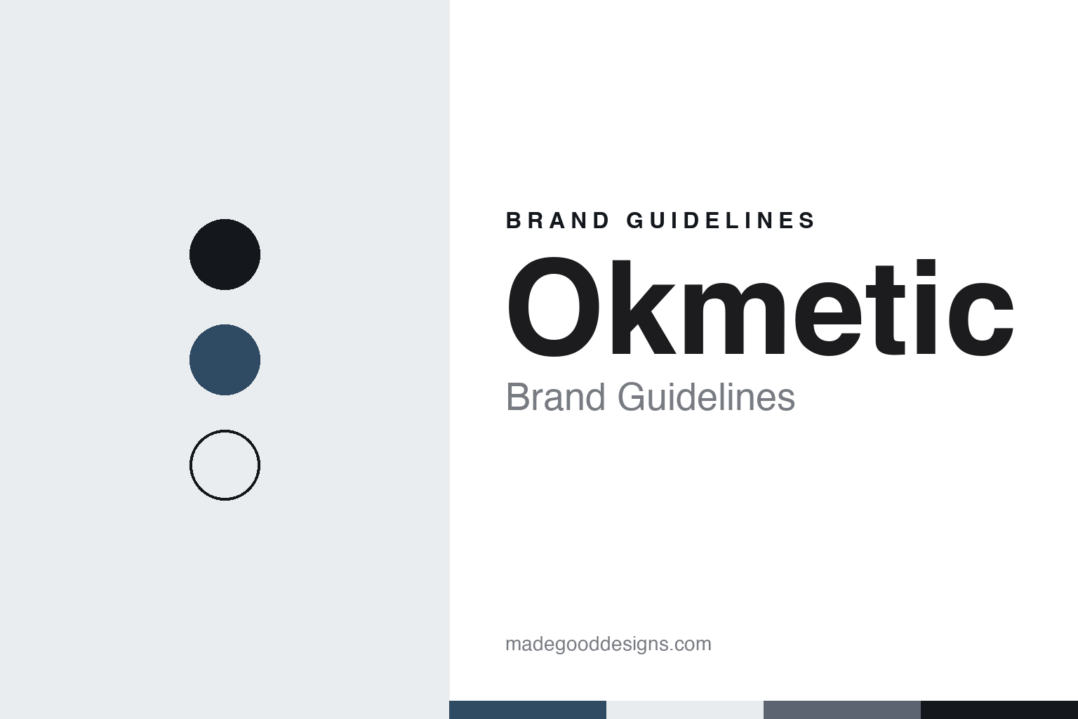
Two constants: an Okmetic blue and wafer grey palette and an Engineered sans register. Abstract homage — not an Okmetic product or mark; no wafer, logo or nameplate is reproduced.
Nokia and Outokumpu
A wafer maker born from a university laboratory.
Okmetic is a Finnish maker of silicon wafers, the thin discs of single-crystal silicon on which chips and sensors are built. It was founded in 1985 as a joint venture of Nokia and Outokumpu, which the company itself describes as the mobile phone company and the mining company. English Wikipedia says the business grew out of research and pilot production of silicon crystals at the Helsinki University of Technology in the late 1970s and early 1980s, with early support from Finland’s Ministry of Trade and Industry, and dates the founding to March 1985, with the company’s registration completed that May.
Its first crystal-growth and wafer plant opened in Espoo in 1987. Ten years later, in 1997, crystal and wafer production started in Vantaa, the city just north of Helsinki that became the company’s main production site and is now its headquarters. Sales offices followed abroad: Okmetic Inc. in the United States in 1999, Okmetic K.K. in Japan in 2006, an Asia-Pacific office in 2011, and offices in Germany in 2019, France in 2023 and Singapore in 2024, according to the company’s own timeline.
Okmetic listed its shares on the Helsinki Stock Exchange in 2000. Finnish Wikipedia says Outokumpu held about 28 per cent of the shares after the listing and 32 per cent at the end of April 2006, roughly halved that stake in May 2006, and sold the rest in November 2010. In 2001 the company began volume production of silicon-on-insulator, or SOI, wafers, in which a thin silicon layer sits on an insulating layer; English Wikipedia says that technology became central to its role as a specialty supplier for MEMS, sensors and radio-frequency devices.
Colour
A new owner in 2016.
The ownership changed in 2016. On 1 April 2016 Okmetic announced that it had received a takeover offer from China’s National Silicon Industry Group, or NSIG, and its board unanimously recommended that shareholders accept it, ScandAsia reported on 10 April 2016. The magazine described NSIG as an industry holding company in China focused on investment in semiconductor equipment and materials, owned by five shareholders, among them China’s National Integrated Circuit Industry Investment Fund and several Shanghai investment groups.
The offer was made through a Finnish subsidiary, NSIG Finland. In a stock exchange release on 10 June 2016, Okmetic said NSIG Finland had obtained confirmation for the offer from Finland’s Ministry of Employment and the Economy. A further release on 7 July 2016 gave the final result: after the subsequent offer period, NSIG Finland would hold about 96.8 per cent of Okmetic’s shares and votes. Finnish Wikipedia says the shares left the stock exchange in November 2016. English Wikipedia says NSIG kept Okmetic’s existing management and committed to keeping its operations and workforce in Finland.
Okmetic makes wafers of 150 and 200 millimetres in diameter at Vantaa: single-side and double-side polished wafers, bonded SOI wafers and Cavity SOI wafers, which it sells as C-SOI, patterned wafers, high-resistivity wafers for radio-frequency devices sold under the name RFSi, and wafers for power devices. Its 300-millimetre wafers and epitaxial wafers come from manufacturing partners, the company says, and English Wikipedia adds contract manufacturing in Japan and China.
Its customers are chipmakers producing MEMS, sensors, radio-frequency and power devices as well as memory, logic and mixed-signal circuits, the company says, and it lists smartphones, cars, industrial and healthcare systems, data centres and energy systems among the end uses. It sells from Finland, Germany, France, the United States, Japan, Singapore and China, with sales agents in Korea and Taiwan.
Typography
Design and documentation.
Silicon-wafer and chip-materials makers sell to a small number of very large customers, and their public image is built for engineers, investors and recruits rather than shoppers. Most of what they make never reaches a consumer’s hand: a polished wafer, a bottle of photoresist or a photomask is used up or hidden inside a chip long before anything is sold in a shop.
Their pictures tend to come from the factory floor. Corporate reports and websites in this field favour mirror-polished silicon wafers catching the light of a cleanroom, cylindrical crystal ingots drawn slowly out of a furnace, photolithography bays lit in amber to protect light-sensitive resists, and racks of high-purity chemical bottles. People appear mostly as technicians in full-body cleanroom suits, often called bunny suits, with only their eyes showing.
Names in this group often record a history. Shin-Etsu joins two old Japanese provinces, and SUMCO is an acronym of the company formed by a 1999 merger. The palettes in these guides are our own interpretations, not official colours.
The industry meets at its trade shows. SEMICON West in the United States, SEMICON Taiwan in Taipei and SEMICON Japan in Tokyo bring wafer, chemical and equipment suppliers onto the same floor as chipmakers, and booths there show the same vocabulary of wafers, ingots and cleanroom imagery. This guide sets out what can be checked about each company — who founded it, who owns it, where it makes its products — and marks clearly what rests only on the company’s own word.
Aa
An engineered sans — a Finnish wafer maker’s plain register. (Specimen set in Inter Tight, a sans STAND-IN; NOT the Okmetic logo.)
Okmetic
Vantaa, enlarged.
Since the change of owner the Vantaa plant has grown. The company says construction work at the plant started in 2017, that between 2017 and 2021 it added capacity for 200-millimetre, SOI, patterned and RFSi wafers, and that in 2019 it moved all C-SOI production to Vantaa. In May 2022 it announced a fab expansion at Vantaa, which it calls the largest investment in its history. Finnish Wikipedia says the new plant would double production capacity and create more than 500 jobs.
The company says the extension was completed in early 2025 and produced its first wafers in June 2025. It covers more than 40,000 square metres, including about 6,000 square metres of cleanroom along with dedicated crystal-growth and wafering areas, and was built onto the existing fab; the original plant continues with 150 and 200 mm polished and bonded SOI wafers and crystal growth. In 2026 the company announced that the expansion had entered volume production. It now describes itself as an EU-based supplier of 150 and 200 mm wafers for the MEMS, radio-frequency and power markets.
Okmetic describes itself in confident terms. Its history page says it is the seventh-largest silicon wafer manufacturer in the world, and its company page is titled “Okmetic is the market leader of advanced silicon wafers”; both are the company’s own claims. Its website is published in English, Finnish and Japanese, and its milestones run from the Espoo plant of 1987 to the Vantaa expansion.
For a design guide, Okmetic shows how a specialist supplier can build an identity on one place and one material: a Finnish plant, and silicon cut and polished there for four decades. Compare Siltronic, the Munich wafer maker, and Soitec, the French SOI specialist. For this guide we use a Nordic blue and a wafer grey with a sans, an unofficial interpretation; no product or logo is reproduced.
Explore & save
Keep Okmetic’s identity on hand — save it to a board in the Made Good inspiration library.
Okmetic identity set
Pin the Okmetic blue and wafer grey palette and the Engineered sans register to your own board.