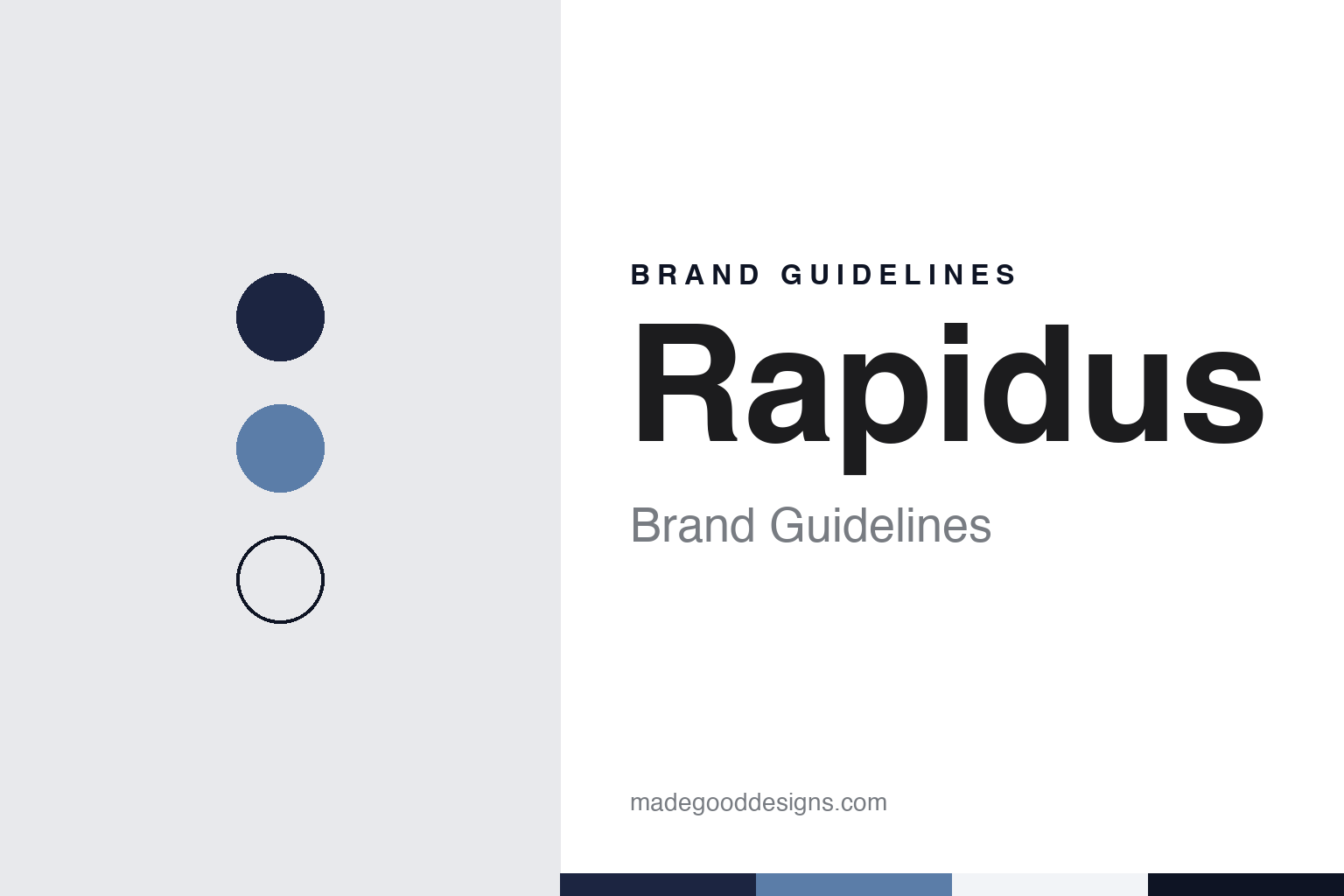
Rapidus Brand Guidelines
Japan’s 2022 chip startup, built around one idea: speed.
Aa
Two constants: a Rapidus indigo, steel and snow palette and a Geometric sans register. Abstract homage — not a Rapidus product or mark; no chip, logo or emblem is reproduced.
A Latin name
Founders, engineers and eight backers.
Rapidus is a Japanese company set up to manufacture leading-edge logic semiconductors, with its head office in Chiyoda, Tokyo, and its production base in Chitose, Hokkaido. Japanese Wikipedia dates its founding to 10 August 2022 and counts twelve founding individual shareholders. The engineering news site MONOist reported in November 2022 that the company’s president, Atsuyoshi Koike, and its chairman, Tetsuro Higashi, had come together with semiconductor engineers through study groups about the industry’s future and became founding shareholders, and that eight companies — Kioxia, Sony Group, SoftBank, Denso, Toyota, NEC, NTT and MUFG Bank — then invested. Japanese Wikipedia dates that corporate investment to 31 October 2022.
The two leaders came from the equipment and chip industries. Higashi formerly led Tokyo Electron, the company’s website says; Koike, MONOist reported, worked on semiconductors at Hitachi and later led Trecenti Technologies and Western Digital’s Japanese business. In a July 2023 interview with Nippon.com, Koike said IBM approached Higashi in the summer of 2020 about manufacturing its 2-nanometre chip technology in Japan, and that Higashi then brought him in and the two talked with the Ministry of Economy, Trade and Industry. He described Trecenti, a Hitachi and UMC joint venture he launched in 2000, as a logic foundry that showed it could halve standard lead times with single-wafer processing.
The name is Latin. MONOist said “Rapidus” comes from the Latin for “rapid” and signals the company’s emphasis on speed; Japanese Wikipedia adds that Koike chose it, and that the logo is meant to evoke Mount Fuji. In November 2022 the ministry chose Rapidus for its project to build a production base for next-generation chips, alongside a new research body, the Leading-edge Semiconductor Technology Center (LSTC), which Higashi also chairs, MONOist reported. Koike told Nippon.com that the company aimed to serve customers with medium-batch needs and to act as a neutral foundry.
Colour
IBM, imec and Chitose.
Rapidus did not start from a process of its own. On 13 December 2022 it announced a joint development partnership with IBM, whose 2-nanometre gate-all-around (GAA) transistor technology it planned to bring into production; a week earlier, on 6 December, it had signed a memorandum of cooperation with imec, the Belgian research centre, and in 2023 it joined imec’s core partner programme, according to English and Japanese Wikipedia. A March 2024 feature in the Japanese government’s Kizuna series said about 100 Rapidus engineers had been sent to IBM’s Albany NanoTech Complex in New York to develop mass-production technology with IBM.
The fab is called IIM-1, short for Innovative Integration for Manufacturing. Japanese Wikipedia says the company chose a site in Chitose’s Bibi World industrial park in February 2023, and groundbreaking took place on 1 September 2023. In December 2024 Rapidus announced the installation of an ASML NXE:3800E extreme-ultraviolet lithography tool there, which it described as the first EUV equipment used for mass production in Japan. Its pilot line began in April 2025, and on 18 July 2025 it announced that prototyping of 2-nanometre GAA transistors had begun at IIM-1 and that it had started measuring electrical characteristics on the prototype wafers.
The company frames its approach around speed. IIM-1 runs fully single-wafer front-end processing, which Rapidus says gives more data for AI models to improve yields, and it brands its service as the Rapid and Unified Manufacturing Service. The Kizuna feature quoted a Rapidus manager comparing the planned turnaround to the difference between a regular slow train and a bullet train. Back-end work sits close by: Rapidus Chiplet Solutions, a packaging research centre set up from October 2024 inside Seiko Epson’s Chitose plant, and an Analysis Center next to IIM-1 both opened on 11 April 2026, the company says.
Typography
Foundries and documentation.
Contract chip makers sell a service rather than a product with their own name on it. The chips they make leave the plant under their customers’ names, so a foundry’s identity has to be built from the things it can show: the wafer, the cleanroom, the fab and the people who run it.
The wafer is the usual starting point. Foundry photographs often show a finished wafer held up to the light, its grid of chips throwing back a rainbow sheen, or a stack of wafers in a carrier ready for the next step. Close-ups of patterned silicon give a company a recognisable image without revealing any customer’s design.
Inside the fab, the pictures follow a familiar pattern: engineers in full-body cleanroom suits, often called bunny suits, standing at tools under the yellow light used in lithography areas; long, bright corridors lined with equipment; and overhead transport systems carrying wafer pods along tracks in the ceiling. From outside, aerial shots of fab campuses, with their long, low buildings and utility plants, stand in for scale and capacity.
Foundries also present themselves at trade shows and conferences, such as the SEMICON exhibitions held in several regions, as well as through their own technology events for customers. Their names usually travel as abbreviations or short forms, and their written materials lean on process names, node figures and fab locations. This guide sets out what can be checked about each company — who founded it, who owns it, where it makes wafers — and marks clearly what rests only on the company’s own word.
Aa
A geometric sans — a Latin name for speed. (Specimen set in Space Grotesk, a sans STAND-IN; NOT the Rapidus logo.)
Rapidus
Mass production planned for 2027.
Rapidus is still preparing for volume production. In its April 2026 announcement it described the new Chitose facilities as steps towards mass production in 2027, the same target year the Kizuna feature gave in 2024. In November 2025 the ministry selected Rapidus as the official operator for the stable production of advanced semiconductors under Japan’s information-processing law, and in February 2026 the company announced a funding round from the government, through the Information-Technology Promotion Agency, and from 32 private companies including Canon, Fujitsu, NTT and Sony Group. Japanese Wikipedia says the government became the largest shareholder but limited its voting rights to 11.5 percent, while holding a golden share with a veto over major decisions. The agency added further equity in June 2026, the company says.
Its customer base is still forming. In February 2024 the Canadian AI-chip company Tenstorrent became its first publicly announced customer, according to English and Japanese Wikipedia. In April 2024 Rapidus set up a US subsidiary, Rapidus Design Solutions, in Silicon Valley, with Henri Richard as president. In October 2026 it launched Rapidus CORE, a framework that began with 17 design-services companies, and opened two HCLTech development centres in Bengaluru and Hubli, India, for work including mask design and process design kits, the company says. Its website gives a headcount of 1,024 as of December 2025.
For a design guide, Rapidus shows how a new company can build its identity around one idea, from a Latin name meaning speed to a fab that processes one wafer at a time. Compare ASML, which supplied its EUV lithography tool, and TSMC, another contract chipmaker. For this guide we use a midnight indigo, a steel blue and a snow white with a sans, an unofficial interpretation; no product or logo is reproduced.
Explore & save
Keep Rapidus’s identity on hand — save it to a board in the Made Good inspiration library.
Rapidus identity set
Pin the Rapidus indigo, steel and snow palette and the Geometric sans register to your own board.