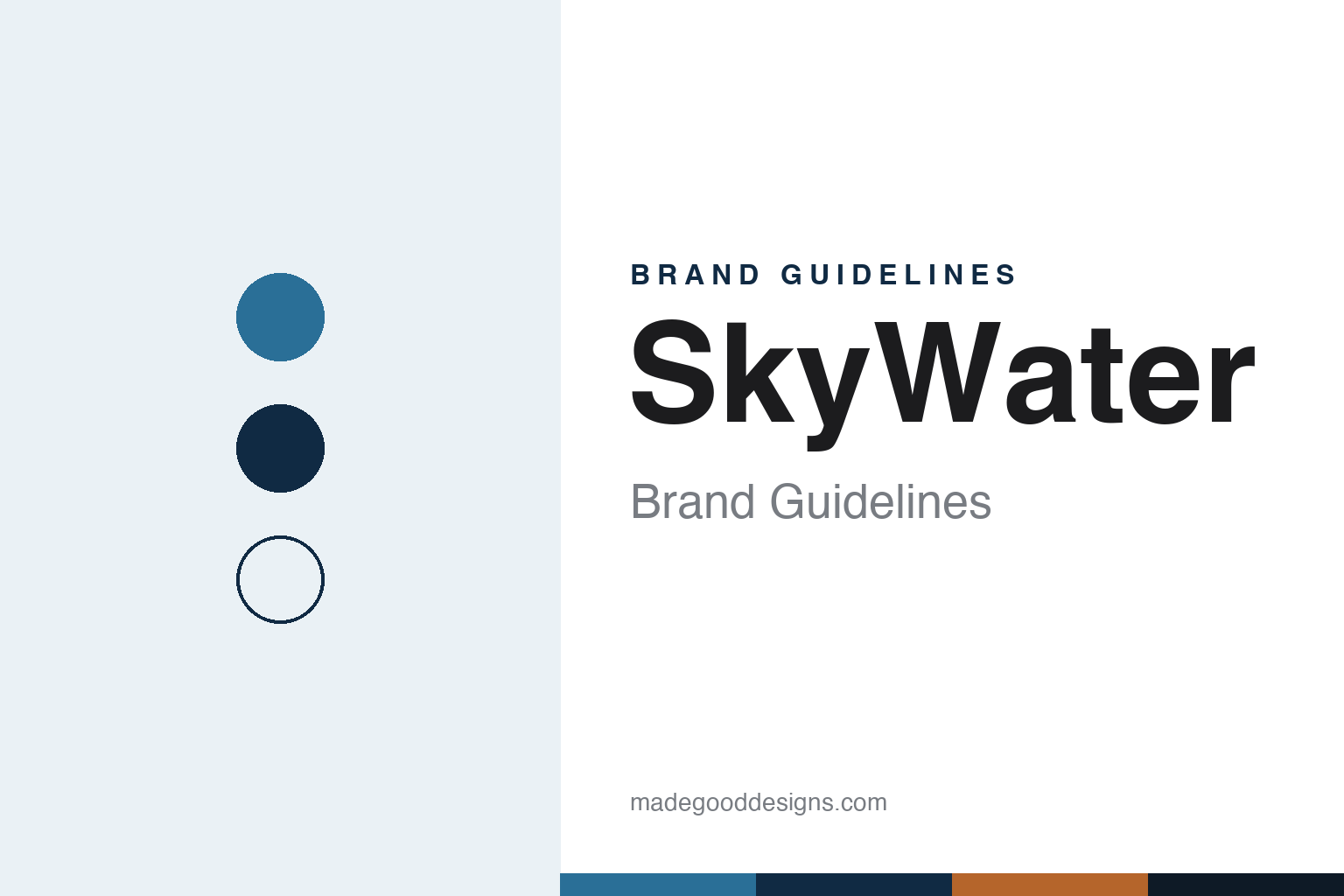
SkyWater Brand Guidelines
The Minnesota foundry built from a Cypress fab.
Aa
Two constants: a lake blue, navy and copper palette and a grotesque sans register. Abstract homage — not a SkyWater product or mark; no wafer, logo or nameplate is reproduced.
A Cypress fab in Bloomington
A Minnesota plant under a new name.
SkyWater began with a factory that already existed. On 27 March 2017 SkyWater Technology Foundry announced that it had acquired Cypress Minnesota Inc., a 200 mm semiconductor wafer fab in Bloomington, Minnesota, from Cypress Semiconductor, with funding from Oxbow Industries, a Minnesota private-equity firm and holding company. The company said the deal kept about 400 manufacturing jobs in the Twin Cities and that it would go on making wafers for Cypress under a multi-year supply agreement while taking work from other customers, including the US government. English Wikipedia dates the company’s formation to that 2017 purchase.
Accounts of the plant’s own origins differ. The 2017 announcement said the facility had originally been commissioned by Control Data Corporation in the 1980s; SkyWater’s current website says the fab was established by Cypress Semiconductor in 1991. Electronics Weekly, writing in March 2021, described it simply as “an old Cypress fab in Minnesota.”
From the start SkyWater presented itself as a Trusted foundry, accredited for US defence work. The 2017 release called it a DMEA-trusted, independent, US-based and US-owned foundry, and Electronics Weekly reported in 2021 that the Department of Defense had invested in SkyWater under its Trusted and Assured Microelectronics programme, which seeks secure sources of chips for the department’s needs.
Colour
An open process, a packaging site and a listing.
SkyWater became known well beyond defence circles through an open-source project. In July 2020 Hackster.io reported that Google and SkyWater had released an open-source process design kit, the rules and files designers need to lay out a chip for a particular factory, for SkyWater’s SKY130 process, which the article described as a hybrid 180–130 nm technology originally developed at Cypress. To encourage its use, Google partnered with the chip-design platform efabless to run manufacturing rounds that built open hardware designs free of charge. SkyWater and Efabless announced in April 2021 the first of these Google-sponsored shuttle runs, with all 40 places filled by open-source designs made at no cost to their designers.
The company then added a second site. In January 2021 SkyWater said it had set up a subsidiary, SkyWater Florida, to take over the Center for NeoVation in Osceola County, Florida, a 200 mm facility with about 36,000 square feet of cleanroom, in partnership with the non-profit BRIDG, to build an advanced packaging business. Its website now lists the site under Kissimmee.
In March 2021 SkyWater filed to go public, Electronics Weekly reported, and its shares began trading on the Nasdaq Capital Market on 21 April 2021 under the symbol SKYT, the company announced. English Wikipedia notes that on 12 April 2021 President Joe Biden held up a silicon wafer made by SkyWater while describing chips as a form of infrastructure. It also records that in July 2022 the company announced plans for a manufacturing facility in West Lafayette, Indiana, in Purdue University’s Discovery Park District, and later withdrew from them for lack of funding.
Its website groups its work under CMOS, radiation-hardened processes for “extreme environments,” MEMS, silicon-nitride photonics under the SP90 name, superconducting processes for quantum computing and sensing, readout chips for infrared sensors and advanced packaging. It gives the Bloomington fab’s geometries as 90 nm and above.
Typography
How foundries present themselves.
Contract chip makers sell a service rather than a product with their own name on it. The chips they make leave the plant under their customers’ names, so a foundry’s identity has to be built from the things it can show: the wafer, the cleanroom, the fab and the people who run it.
The wafer is the usual starting point. Foundry photographs often show a finished wafer held up to the light, its grid of chips throwing back a rainbow sheen, or a stack of wafers in a carrier ready for the next step. Close-ups of patterned silicon give a company a recognisable image without revealing any customer’s design.
Inside the fab, the pictures follow a familiar pattern: engineers in full-body cleanroom suits, often called bunny suits, standing at tools under the yellow light used in lithography areas; long, bright corridors lined with equipment; and overhead transport systems carrying wafer pods along tracks in the ceiling. From outside, aerial shots of fab campuses, with their long, low buildings and utility plants, stand in for scale and capacity.
Foundries also present themselves at trade shows and conferences, such as the SEMICON exhibitions held in several regions, as well as through their own technology events for customers. Their names usually travel as abbreviations or short forms, and their written materials lean on process names, node figures and fab locations. This guide sets out what can be checked about each company — who founded it, who owns it, where it makes wafers — and marks clearly what rests only on the company’s own word.
Aa
A sturdy grotesque for an industrial foundry. (Specimen set in Archivo, a sans STAND-IN; NOT the SkyWater logo.)
SkyWater
From Fab 25 to IonQ.
In 2025 SkyWater grew by buying another company’s fab. On 26 February 2025 it announced an agreement with Infineon Technologies to buy Infineon’s 200 mm fab in Austin, Texas, known as Fab 25, together with a long-term agreement to keep supplying Infineon. SkyWater said it would run the plant as a foundry for chips on nodes from 130 down to 65 nanometres, adding copper processing and high-voltage BCD technology, and that the fab’s employees, nearly 1,000 people, would join SkyWater. The company announced on 30 June 2025 that the purchase was complete, describing it as turning a factory that had served one chipmaker into an open-access foundry and putting the added capacity at about 400,000 wafer starts a year; English Wikipedia gives the same completion date.
The next change was in ownership. On 26 January 2026 SkyWater and the quantum-computing company IonQ announced a definitive agreement for IonQ to acquire SkyWater in a cash-and-stock deal, and on 31 July 2026 the companies announced that the acquisition was complete after the required regulatory approvals. SkyWater now operates as an IonQ subsidiary under the SkyWater name, led by its existing chief executive, and says it continues to serve its other foundry customers. In October 2026 it announced a multi-year agreement with the quantum-computing company D-Wave, extending a long-running manufacturing partnership at the Minnesota fab.
SkyWater describes itself as the largest exclusively US-based semiconductor foundry; that is the company’s own claim. Its website lists three facilities: the Bloomington headquarters fab, the Florida packaging site and Fab 25 in Austin, which it gives as 65 nm and above.
For a design guide, SkyWater shows how a regional plant can be rebuilt as a national brand around trust, open tools and domestic manufacturing. Compare GlobalFoundries, another US-based contract chipmaker, and Tower Semiconductor, a specialty foundry. For this guide we use a lake blue, a deep navy and a copper accent with a sans, an unofficial interpretation; no product or logo is reproduced.
Explore & save
Keep SkyWater’s identity on hand — save it to a board in the Made Good inspiration library.
SkyWater identity set
Pin the SkyWater lake blue, navy and copper palette and the grotesque sans register to your own board.