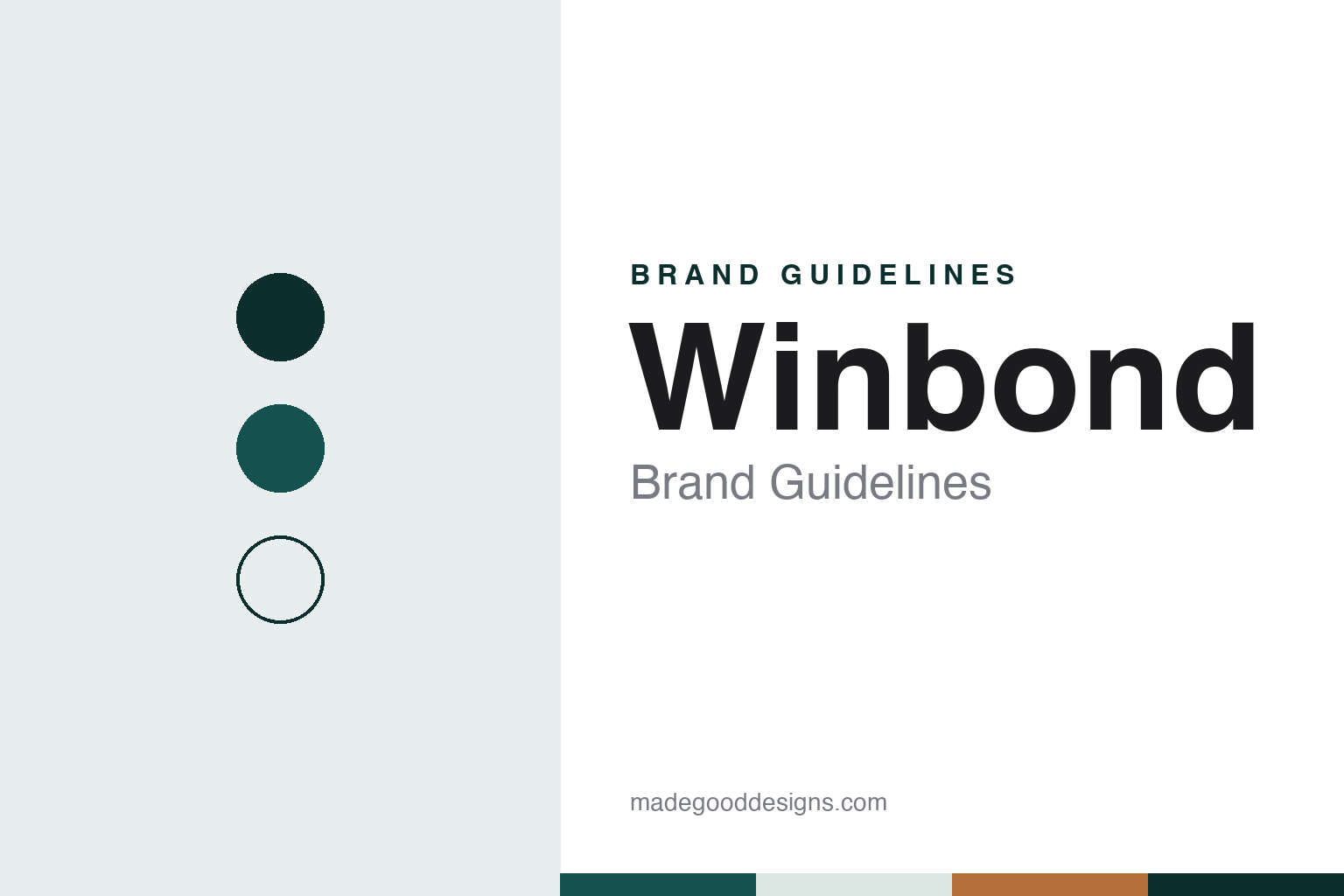
Winbond Brand Guidelines
From a research-institute spin-off to specialty DRAM and flash.
Aa
Two constants: a deep teal, silicon mist and copper palette and a rounded geometric sans register. Abstract homage — not a Winbond product or mark; no chip, package, logo or nameplate is reproduced.
An ERSO spin-off
Eight engineers, a lab and a CMOS licence.
Winbond Electronics was founded in September 1987, the company says. The International Directory of Company Histories, in a 2006 profile republished by Reference for Business, names its founder as Ding-yuan Yang, a founding member of ERSO, the electronics research organisation of Taiwan’s Industrial Technology Research Institute, who left with seven other ERSO engineers. Yang lined up an investor, Walsin Lihwa Corporation, and set up the company. The profile says Winbond, unlike the earlier ERSO offshoots TSMC and UMC, was not directly controlled by ERSO but drew on its support: the use of ERSO’s original laboratory in Hsinchu, a further team of 40 engineers, and a licence for ERSO’s CMOS chip technology.
The early company made logic chips before memory. English Wikipedia says its first fab, built in 14 months over 1987 and 1988 in the Hsinchu Science Park, produced 6-inch wafers, and that a second fab followed between 1989 and 1992. The 2006 profile describes chipsets for Intel’s 286, 386 and 486 processors, video-display controllers, voice and early multimedia chips from 1989, and a first chip for LCD screens in 1990, the year subsidiaries opened in the United States and Hong Kong. It says Winbond developed the first single-chip MPEG video decoder designed in Asia in 1994. English Wikipedia adds that in October 1995 Winbond bought Symphony Laboratories, a chipset maker in San Jose, California.
Winbond listed on the Taiwan Stock Exchange in 1995, the same year its second fab was completed, according to the profile.
Colour
From Toshiba to Qimonda, and its own processes.
Memory came through partners. After the listing, the 2006 profile says, Winbond signed a licence with Toshiba to design and produce DRAM and high-speed SRAM chips. Its third fab, completed in May 1996, was destroyed by fire later that year; a fourth fab began pilot production of 64M DRAM based on Toshiba technology by the end of 1997. Acquisitions in the United States added voice-recording chips, through Information Storage Devices in 1998, and flash memory design, through NexFlash Technologies, which Winbond fully controlled from June 2005.
When Toshiba left the DRAM business in the early 2000s, Winbond turned to Germany’s Infineon, signing a technology agreement in 2002 and expanding it in 2004, when it began building a new 12-inch fab, according to the profile. Infineon’s memory arm became Qimonda in 2006; English Wikipedia says that in 2010 Winbond was making DDR2 DRAM with technology licensed from Qimonda. Chinese-language Wikipedia says that after Qimonda left the market in 2009, Winbond bought its patents and used them as the basis for its own process development, moving towards specialty memory rather than mainstream computer DRAM.
The company also narrowed its scope. On 1 July 2008 its computer chip, consumer electronics chip and logic foundry divisions were spun off as Nuvoton Technology, English Wikipedia says. In August 2026 the Taipei Times still described Nuvoton as a Winbond subsidiary, with its logic-chip business reported inside the group’s results.
Winbond now names its main lines as Code Storage Flash, TrustME Secure Flash, a Customized Memory Solution business and logic chips. Its product pages list pseudo-SRAM, DDR and low-power DRAM, known-good die, NOR flash in serial, Quad SPI and Octal forms, and NAND flash. In September 2023 it introduced CUBE, a memory architecture it presents for edge AI devices. Its milestones list 20-nanometre DRAM in volume production from August 2023, 24-nanometre NAND flash from January 2025 and verification of a 16-nanometre DRAM in September 2025, all on processes it says it developed itself.
Typography
Design and documentation.
Memory chips are hard to show. A finished DRAM or flash die is a sliver of silicon sealed inside a black package, and the companies that make them sell mostly to other manufacturers rather than to the public. So memory makers tend to build their visual identity from the stages around the chip: the wafer, the module, the drive and the place where it all ends up.
The wafer is the most common image. A polished disc covered in a tight grid of identical dies, often lit so that the surface breaks into bands of colour, says “scale” and “precision” without needing a product name. Close-ups follow the chip outward: DRAM modules with rows of packages along a green board, SSD circuit boards with a controller and flash packages side by side, and cross-section diagrams that show memory cells stacked in layers, the shorthand for 3D NAND.
The factory is the second theme. Cleanroom corridors, staff in full-body suits and long rows of wafer-handling equipment appear in annual reports, recruitment pages and listing documents, usually photographed in cool, even light. At the other end of the chain come data-centre racks, banks of servers and drives that show where the memory is put to work.
Trade shows give the category its public stage. Memory and storage makers present new parts at events such as FMS, the Flash Memory Summit, and Computex in Taipei, where stands mix wafer displays, product cases and technical posters. Across these settings the typical register is a clean sans, a cool or dark palette with one bright accent, and diagrams in place of lifestyle photography; the guides in this series look at how each maker works within, or departs from, that pattern.
Aa
A rounded geometric sans — the register of a specialty memory maker. (Specimen set in Manrope, a sans STAND-IN; NOT the Winbond logo.)
Winbond
Two fabs, Taichung and Kaohsiung.
Winbond is headquartered in the Central Taiwan Science Park in Taichung and runs two 12-inch fabs, one there and one in the Kaohsiung Science Park, part of the Southern Taiwan Science Park, the company says. It describes the Kaohsiung plant as its second 12-inch fab, and says its groundbreaking was hosted by chairman and chief executive Arthur Yu-Cheng Chiao. In September 2021 the Taipei Times, calling Winbond “Taichung-based,” reported that the Kaohsiung fab was due to make DRAM in small volumes from July 2022 ahead of regular production that October, with a target of 35,000 wafers a month, and that the company was hiring engineers for sites in Kaohsiung, Taichung, Hsinchu and Taipei.
In August 2026 the same paper reported that Winbond planned to start building a second phase at Kaohsiung, called Module B, in January 2027, with pilot production set for the end of 2029 and extreme ultraviolet lithography planned for later phases. Its NOR and NAND flash are mostly made at the Taichung fab, the paper said. Winbond president James Chen told the Taipei Times: “I never thought we would need EUV equipment. Now we want to buy” a machine.
The company’s own description is broad. Winbond calls itself one of the few companies with its own products and technology in both memory and logic chips, says its goal is to become “a hidden champion” in semiconductors, and lists operations and distributor networks in the United States, China, Japan, Germany, India, Korea, Hong Kong, Singapore and Israel. It says it was the first memory maker in Taiwan to obtain ISO 26262 certification, the automotive functional-safety standard, and names cars and industrial electronics among its focus markets.
For a design guide, Winbond shows how a research-institute spin-off can rebuild itself around a narrow product niche after its technology partners leave the market. Compare Nanya Technology, another Taiwanese DRAM maker that moved from licensed processes to its own, and Toshiba, its first DRAM partner. For this guide we use a deep teal, a silicon mist and a copper with a sans, an unofficial interpretation; no product or logo is reproduced.
Explore & save
Keep Winbond’s identity on hand — save it to a board in the Made Good inspiration library.
Winbond identity set
Pin the Winbond deep teal, silicon mist and copper palette and the rounded geometric sans register to your own board.