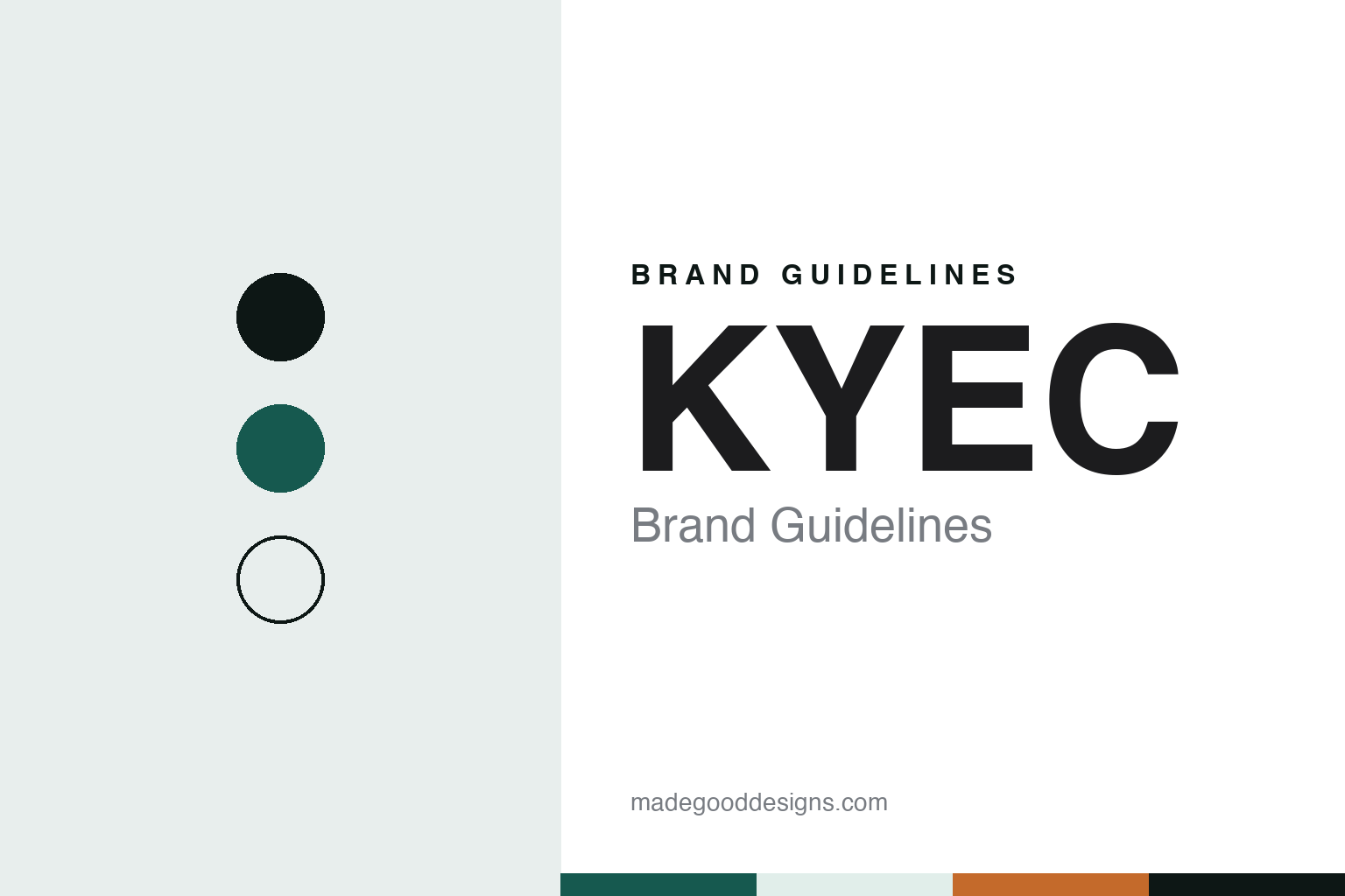
KYEC Brand Guidelines
The Hsinchu chip-testing house founded in 1987.
Aa
Two constants: a KYEC green, mint and amber palette and a Technical sans register. Abstract homage — not a KYEC product or mark; no test system, logo or nameplate is reproduced.
King Yuan Electronics
A Hsinchu company built around the test floor.
KYEC is the short name of King Yuan Electronics Co., Ltd., a Taiwanese company in the back end of chipmaking. The company says it was founded in May 1987 and is headquartered in Hsinchu City; Chinese Wikipedia describes it as a semiconductor packaging and testing company set up in 1987 to provide test and packaging services and capacity for the final stages of chip production around the world.
Chinese Wikipedia gives a short chronology. The Hsinchu headquarters was completed in 2000, and in 2001 the company listed on the Taiwan Stock Exchange. It opened a Singapore branch in 2004 and a Japanese branch in 2006, and in 2018 it merged a joint venture, 東琳精密, into the company. In 2021, Chinese Wikipedia adds, its employees formed a trade union.
The company’s production is in Taiwan’s north-west. It names factory sites in Miaoli County, at Chunan, Tongluo and Toufen, and in Taoyuan, at Yangmei, and keeps sales offices in North America, Japan and Singapore. In December 2024 the Taipei Times reported that King Yuan operated two fabs in Miaoli’s Jhunan and Tongluo townships and had rented a factory shell in Toufen, where it was building a clean room for new equipment.
Colour
Probe, final test and burn-in.
Where many companies in its category both package and test chips, KYEC presents itself around testing. It describes itself as the world’s largest pure-play semiconductor testing company; that is the company’s own claim. Evertiq, in May 2024, called it one of the world’s largest semiconductor testing and packaging services firms.
The company groups its work into four stages. Chip probing takes place after wafer fabrication and before dicing, with probe cards touching each die to sort out faulty ones early. Final test comes after packaging, to check that shipped chips meet their specifications, and the company says it is its largest line of business. Burn-in runs chips for long periods at high temperature and voltage to screen out early failures, and system-level test checks chips under real workloads before they ship. The company says it develops its own equipment for high-power burn-in, and it lists more than 5,900 test systems.
By product, KYEC lists systems-on-chip, logic and mixed-signal devices, CMOS image sensors, LCD drivers, radio-frequency chips and MEMS, for customers in computing, communications, consumer electronics, cars and industry. It says its customers are mostly fabless chip designers, integrated device makers and foundries, that nearly half of the world’s top 50 semiconductor companies use its services, and that its recent growth has come from chips for AI computing.
The company also publishes its own capacity figures. On its 2026 company profile it gives monthly wafer-probing capacity of roughly 350,000 wafers, counted as 12-inch equivalents, and final-test capacity of about 350 million chips a month. It names flexible capacity allocation, quality control, on-time delivery and engineering support as its strengths, and puts its own work on test automation and custom test parts at the centre of them.
The press confirms the AI link. The Taipei Times wrote in December 2024 that King Yuan counted NVIDIA as a key customer, and that most of its planned equipment spending for 2025 would go on final-test equipment and tools such as test handlers, as longer final testing was needed for more complex chips. The company’s stated core values are “Performance, Innovation, Excellence and Sharing.”
Typography
How chip packaging and test companies present themselves.
Chip packaging and test companies sit between the chipmaker and the finished device. The trade calls them OSATs, for outsourced semiconductor assembly and test: they take silicon made by others, mount it, connect it, seal it and check that it works. Their customers are other technology companies, so they rarely speak to the public, and their imagery is built for engineers, buyers and investors.
That imagery leans on close-ups. Company pages and annual reports return again and again to macro shots of packaged chips and the substrates beneath them, to fine arcs of gold or copper wire bonds linking a die to its frame, and to wafers catching the light. Methods carry the names that a consumer brand would give to products: flip chip, fan-out, system in package, 2.5D and chiplet packaging.
The second register is the factory. Rows of test handlers, operators in white cleanroom suits, and long, low factory campuses in places such as Kaohsiung, Penang and Jiangsu stand for scale and reliability. Plants are often known by codes and numbers rather than names, and maps of sites across Asia, Europe and the Americas do much of the storytelling. Trade shows such as SEMICON are where these companies meet their customers face to face.
This guide sets out what can be checked about each company — who founded it, who owns it, where it works and what its record shows — and marks clearly what rests only on the company’s own word. The palettes and type here are our own interpretation, not the companies’ marks.
Aa
A technical sans for a testing house. (Specimen set in IBM Plex Sans, a sans STAND-IN; NOT the KYEC logo.)
KYEC
Out of Suzhou, towards the United States.
KYEC once had a large mainland Chinese operation. On 26 April 2024 it announced that it would sell its entire 92.16 per cent stake in its Suzhou subsidiary, King Long Technology. Evertiq reported on 3 May 2024 that the buyers included investment companies, a Suzhou Industrial Park fund, a Shanghai state-owned enterprise fund and Tongfu Microelectronics, with completion then expected in the third quarter of 2024. KYEC was still reporting the Suzhou business as held for disposal in late 2024, and the reports used for this guide give no completion date. KYEC said that geopolitics, including United States restrictions on China’s semiconductor industry, had changed the operating environment in China and sharpened competition, and that its board had decided to withdraw from China’s semiconductor manufacturing business.
Its expansion since then has pointed elsewhere. The company says it established a testing facility in Singapore in 2026 and plans to build a factory in the United States. On 21 October 2026 NVIDIA announced plans with a group of suppliers, King Yuan among them, to expand manufacturing capacity, saying that KYEC would build new testing facilities in the United States supported by a capacity reservation advance from NVIDIA, with high-volume production targeted for April 2027.
The name needs care. “KYEC” is also the call sign of a radio station in Missouri, and the company itself uses both forms, King Yuan Electronics in full and KYEC for short, alongside its Chinese name, 京元電子.
For a design guide, KYEC shows how a company with no consumer product presents itself through process: probe, test and burn-in, explained step by step. Compare Powertech Technology, another Taiwanese chip packaging and test company, and NVIDIA, whose chips it tests. For this guide we use a deep green, a pale mint and an amber with a sans, an unofficial interpretation; no product or logo is reproduced.
Explore & save
Keep KYEC’s identity on hand — save it to a board in the Made Good inspiration library.
KYEC identity set
Pin the KYEC green, mint and amber palette and the Technical sans register to your own board.